CDP1871 Просмотр технического описания (PDF) - Intersil
Номер в каталоге
Компоненты Описание
Список матч
CDP1871 Datasheet PDF : 10 Pages
| |||

CDP1871A, CDP1871AC
Functional Description of
CDP1871A Terminals
D1 - D11 (Outputs):
Drive lines for the 11 x 8 keyboard switch matrix. These
outputs are connected through the external switch matrix to
the sense lines (S1 - S8).
TPB (Input):
The input clock used to drive the scan generator and reset
the status flag (DA). This input is normally connected to the
TPB output of the CDP1800-series microprocessor.
S1 - S8 (Inputs):
Sense lines for the 11 x 8 keyboard maxtrix. These inputs
have internal pull-down resistors and are driven high by
appropriate drive line when a keyboard switch is closed.
CS1, CS2, CS3, CS4 (Inputs):
Chip select inputs, which are used to enable the three-state
data bus outputs (BUS 0 - BUS 7) and to enable the reset-
ting of the status flag (DA), which occurs on the low-to-high
transition of TPB. These four inputs are normally connected
to the N-lines (N0-N2) and MRD output of the CDP1800-
series microprocessor. (Table 2)
BUS 0 - BUS 7 (Outputs):
Three-state data bus outputs which provide the ASCll and
HEX codes of the detected keys. The outputs are normally
connected to the BUS 0 - BUS 7 terminals of the CDP1800-
series microprocessor.
DA (Output):
The data available output flag which is set low when a valid
key closure is detected. It is reset high by the low-to-high
transition of TPB when data is read from the CDP1871A.
This output is normally connected to a flag input (EF1 - EF4)
of the CDP1800-series microprocessor.
RPT (Output):
The repeat output flag which is used to indicate that a key is
still closed after data has been read from the CDP1871A
(DA = high). It remains low as long as the key is closed and
is used for an autorepeat function, under CPU control. This
output is normally connected to a flag input (EF1 - EF4) of
the CDP1800-series microprocessor.
DEBOUNCE (Input):
This input is connected to the junction of an external resistor
to VDD and capacitor to VSS. It provides a debounce time
delay (t ≅ RC) after the release of a key. If a debounce is not
desired, the external pull-up resistor is still required.
ALPHA, SHIFT, CONTROL (Inputs):
A high on the SHIFT or CONTROL inputs will be internally
latched (after the debounce time) and the drive and sense
line decoding will be modified as shown in Table 3. They are
normally connected to the keyboard, but produce no code by
themselves. The SHIFT and CONTROL inputs have internal
pull-down resistors to simplify use with momentary contact
switches. The ALPHA input is not latched and is designed for
a standard SPDT switch to provide an alpha-lock function.
When ALPHA = 1 the drive and sense line decoding will be
modified as shown in Table 3.
VDD, VSS:
VDD is the positive supply voltage input. VSS is the most
negative supply voltage terminal and is normal connected to
ground. All outputs swing from VSS to VDD. The
recommended input voltage swing is from VSS to VDD.
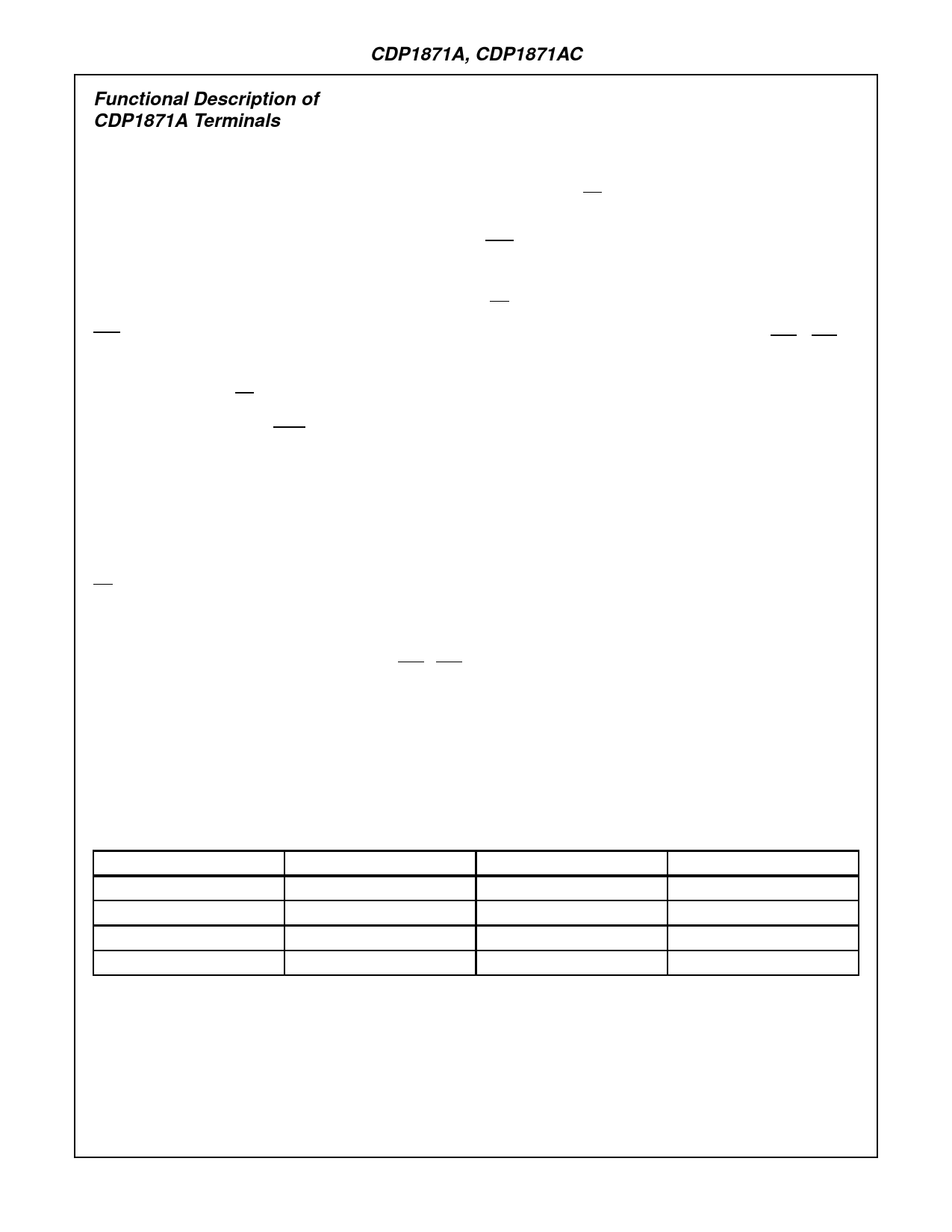
CONTROL
0
1
0
0
NOTE: X = Don’t Care
TABLE 1. SWITCH INPUT FUNCTIONS
SHIFT
0
X
1
0
ALPHA
0
X
X
1
KEY FUNCTION
Normal
Control
Shift
Alpha
4-70