CS4385-CQZ Просмотр технического описания (PDF) - Cirrus Logic
Номер в каталоге
Компоненты Описание
Список матч
CS4385-CQZ Datasheet PDF : 55 Pages
| |||
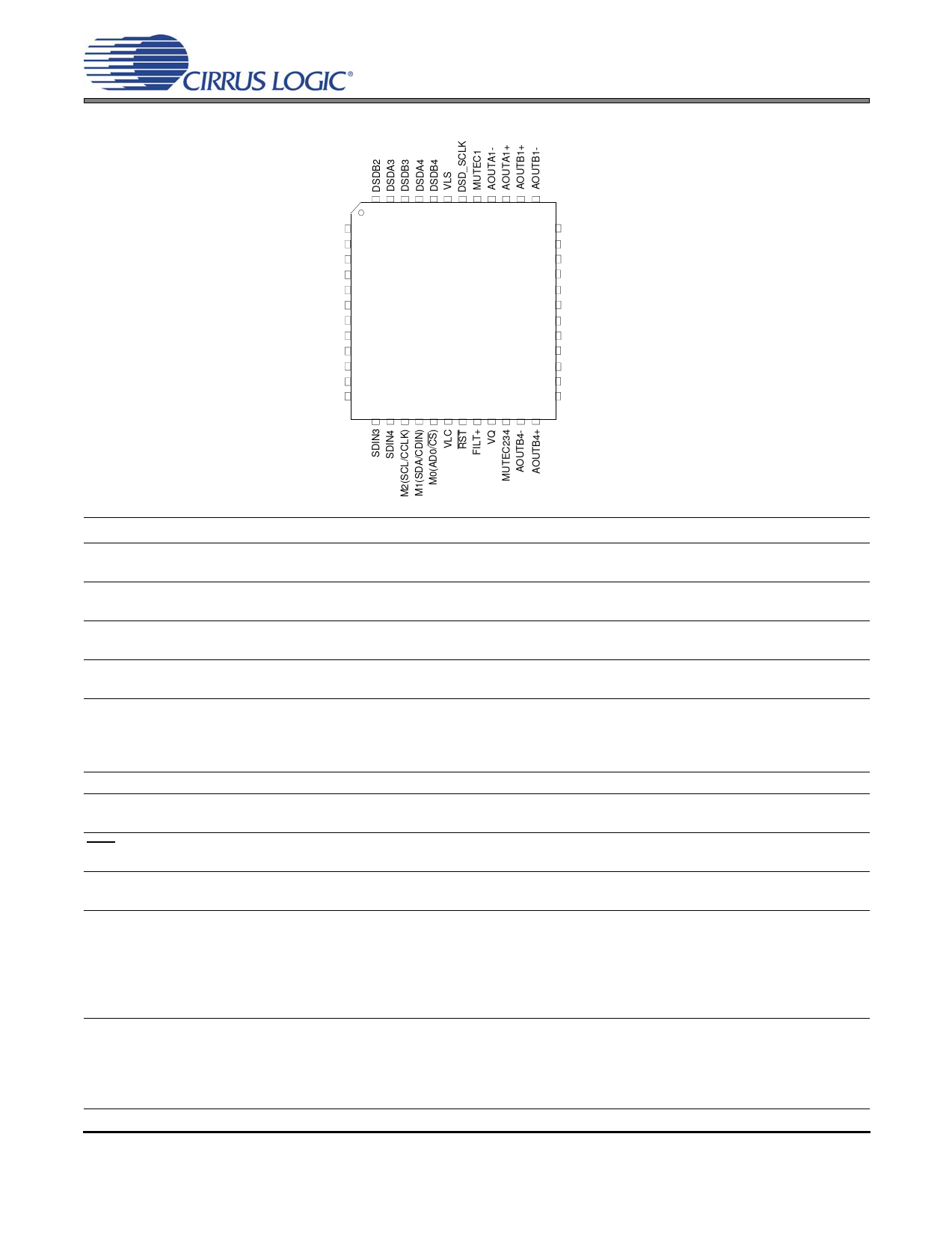
1. PIN DESCRIPTION
DSDA2
DSDB1
DSDA1
VD
GND
MCLK
LRCK
SDIN1
SCLK
M4(TST)
SDIN2
M3(TST)
48 47 46 45 44 43 42 41 40 39 38 37
1
36
2
35
3
34
4
33
5
32
6
CS4385
31
7
30
8
29
9
28
10
27
11
26
12
25
13 14 15 16 17 18 19 20 21 22 23 24
AOUTA2-
AOUTA2+
AOUTB2+
AOUTB2-
VA
GND
AOUTA3-
AOUTA3+
AOUTB3+
AOUTB3-
AOUTA4-
AOUTA4+
CS4385
Pin Name
VD
GND
MCLK
LRCK
SDIN1
SDIN2
SDIN3
SDIN4
SCLK
VLC
RST
FILT+
VQ
MUTEC1
MUTEC234
#
Pin Description
4
Digital Power (Input) - Positive power supply for the digital section. Refer to the Recommended Oper-
ating Conditions for appropriate voltages.
5
31
Ground (Input) - Ground reference. Should be connected to analog ground.
6
Master Clock (Input) - Clock source for the delta-sigma modulator and digital filters. Tables 1-3 illus-
trate several standard audio sample rates and the required master clock frequency.
7
Left Right Clock (Input) - Determines which channel, Left or Right, is currently active on the serial
audio data line. The frequency of the left/right clock must be at the audio sample rate, Fs.
8
11
13
Serial Audio Data Input (Input) - Input for two’s complement serial audio data.
14
9 Serial Clock (Input) - Serial clock for the serial audio interface.
18
Control Port Power (Input) - Determines the required signal level for the control port. Refer to the
Recommended Operating Conditions for appropriate voltages.
19
Reset (Input) - The device enters a low power mode and all internal registers are reset to their default
settings when low.
20
Positive Voltage Reference (Output) - Positive reference voltage for the internal sampling circuits.
Requires the capacitive decoupling to analog ground, as shown in the Typical Connection Diagram.
Quiescent Voltage (Output) - Filter connection for internal quiescent voltage. VQ must be capacitively
coupled to analog ground, as shown in the Typical Connection Diagram. The nominal voltage level is
21
specified in the Analog Characteristics and Specifications section. VQ presents an appreciable source
impedance and any current drawn from this pin will alter device performance. However, VQ can be
used to bias the analog circuitry assuming there is no AC signal component and the DC current is less
than the maximum specified in the Analog Characteristics and Specifications section.
Mute Control (Output) - The Mute Control pins go high during power-up initialization, reset, muting,
41
22
power-down or if the master clock to left/right clock frequency ratio is incorrect. These pins are
intended to be used as a control for external mute circuits to prevent the clicks and pops that can
occur in any single supply system. The use of external mute circuits are not mandatory but may be
desired for designs requiring the absolute minimum in extraneous clicks and pops.
6
DS671F2
Share Link: 