CDB4362(2004) Просмотр технического описания (PDF) - Cirrus Logic
Номер в каталоге
Компоненты Описание
Список матч
CDB4362 Datasheet PDF : 42 Pages
| |||
CS4362
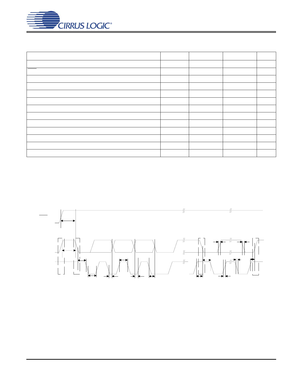
SWITCHING CHARACTERISTICS - CONTROL PORT - SPI™ FORMAT
(For KQZ TA = -10 to +70 °C; VLC = 1.8 V to 5.5 V; Inputs: Logic 0 = GND, Logic 1 = VLC, CL = 30 pF)
Parameter
Symbol
Min
Max
CCLK Clock Frequency
fsclk
-
M------C-----L----K--
2
RST Rising Edge to CS Falling
CCLK Edge to CS Falling
CS High Time Between Transmissions
CS Falling to CCLK Edge
CCLK Low Time
tsrs
500
-
(Note 22)
tspi
500
-
tcsh
1.0
-
tcss
20
-
tscl
--------1---------
-
MCLK
CCLK High Time
tsch
--------1---------
-
MCLK
CDIN to CCLK Rising Setup Time
CCLK Rising to DATA Hold Time
Rise Time of CCLK and CDIN
Fall Time of CCLK and CDIN
tdsu
40
-
(Note 23)
tdh
15
-
(Note 24)
tr2
-
100
(Note 24)
tf2
-
100
Unit
MHz
ns
ns
µs
ns
ns
ns
ns
ns
ns
ns
Notes: 22. tspi only needed before first falling edge of CS after RST rising edge. tspi = 0 at all other times.
23. Data must be held for sufficient time to bridge the transition time of CCLK.
24. For FSCK < 1 MHz.
RST
t srs
CS
t spi t css
t scl t sch
t csh
CCLK
t r2
t f2
C D IN
t dsu t dh
Figure 4. Control Port Timing - SPI Format
DS257F1
11
Share Link: 