CS4361-CZZ(2005) Просмотр технического описания (PDF) - Cirrus Logic
Номер в каталоге
Компоненты Описание
Список матч
CS4361-CZZ Datasheet PDF : 23 Pages
| |||
CS4361
DIGITAL INPUT CHARACTERISTICS
Parameters
Symbol Min Typ Max Units
High-Level Input Voltage -all input Pins except RST (% of VL) VIH
70%
-
-
V
Low-Level Input Voltage -all input Pins except RST (% of VL) VIL
-
-
30%
V
High-Level Input Voltage -RST pin (Note 6)
(% of VL) VIH
90%
-
-
V
Low-Level Input Voltage -RST pin
(% of VL) VIL
-
-
10%
V
Input Leakage Current
(Note 7)
Iin
-
-
±10
µA
Input Capacitance
-
8
-
pF
6. RST pin has an input threshold relative to VL but is VA tolerant.
7. Iin for LRCK is ±20 µA max.
POWER & THERMAL CHARACTERISTICS
Parameters
Symbol
Power Supplies
Power Supply Current
normal operation IA
(Note 8)
IL
power-down state (Note 9) IA
IL
Power Dissipation
normal operation
power-down state (Note 9)
Package Thermal Resistance
θJA
Power Supply Rejection Ratio (Note 10) (1 kHz) PSRR
(60 Hz)
5 V Nom
Min Typ Max
-
66 90
-
0.1
1
- 300 -
-
26
-
- 331 455
- 1.63 -
-
72
-
-
60
-
-
40
-
3.3 V Nom
Min Typ Max Units
-
48 63 mA
-
0.1
1
mA
- 180 -
µA
-
24
-
µA
- 159 211 mW
- 0.67 -
mW
-
72
- °C/Watt
-
60
-
dB
-
40
-
dB
8. Current consumption increases with increasing FS and increasing MCLK. Typ and Max values are
based on highest FS and highest MCLK. Current variance between speed modes is small.
9. Power down mode is defined when all clock and data lines are held static.
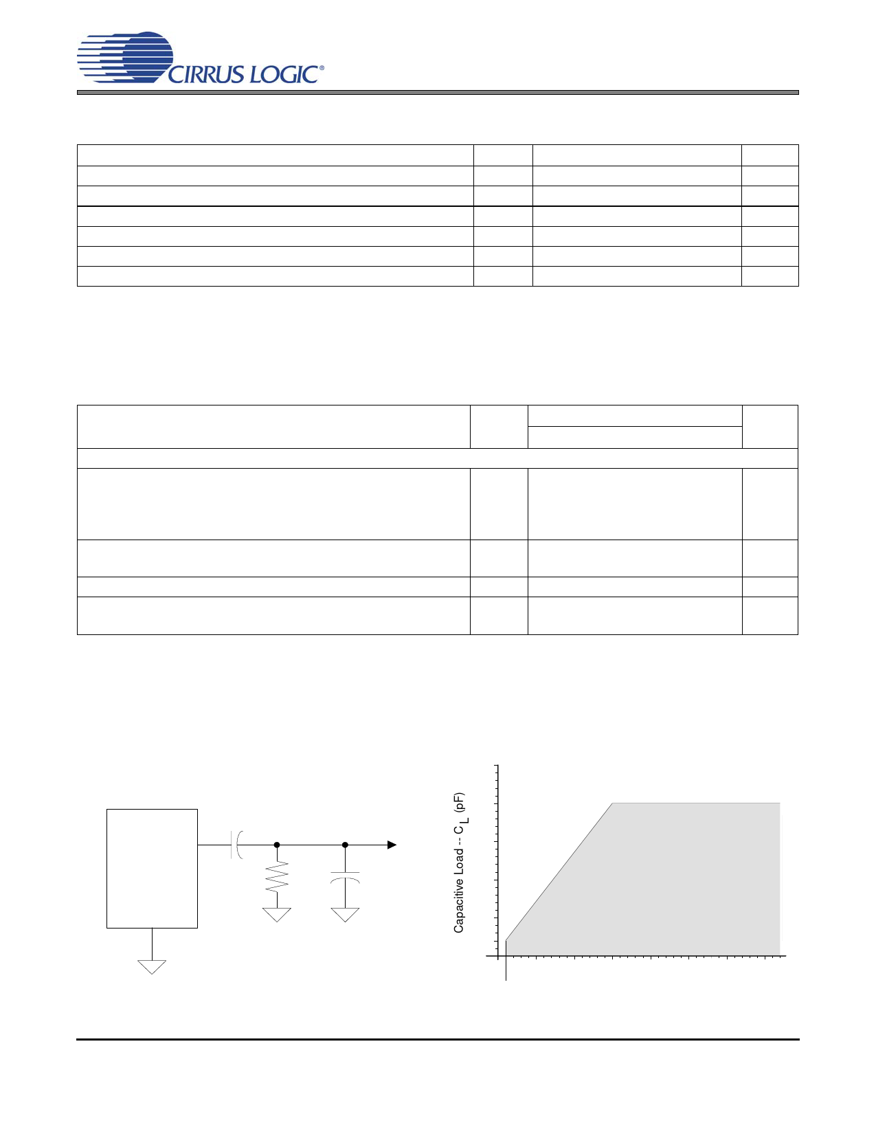
10. Valid with the recommended capacitor values on VQ and FILT+ as shown in the typical connection
diagram in Section 3.
125
AOUTx
3.3 µF
R
L
AGND
Vo ut
C
L
100
75
50
25
Safe Operating
Region
Figure 1. Equivalent Output Test Load
2.5 5
3
10
15
20
Resistive Load -- RL (kΩ )
Figure 2. Maximum Loading
8
DS672A2
Share Link: 