CBT3306 Просмотр технического описания (PDF) - Philips Electronics
Номер в каталоге
Компоненты Описание
Список матч
CBT3306 Datasheet PDF : 8 Pages
| |||
Philips Semiconductors
Dual bus switch
Product data
CBT3306
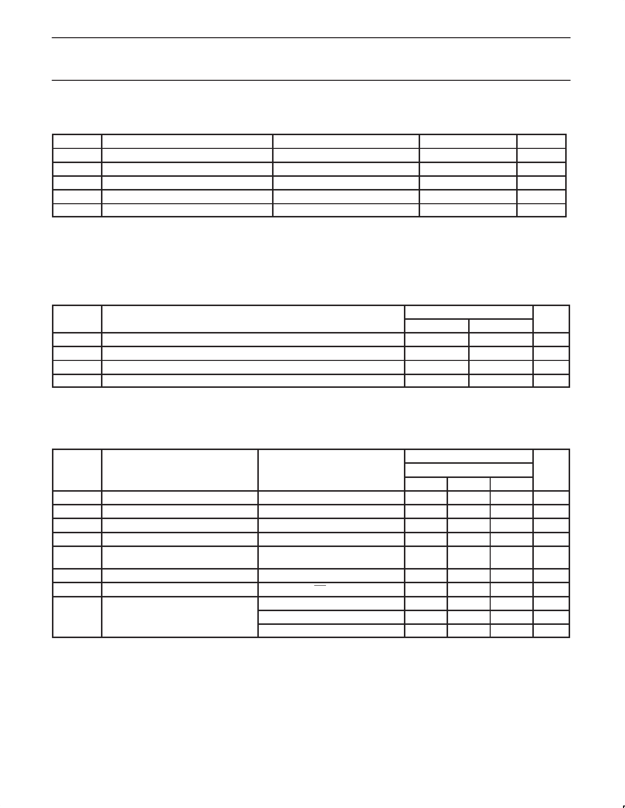
ABSOLUTE MAXIMUM RATINGS1
Tamb = –40 to +85 °C, unless otherwise specified.
SYMBOL
PARAMETER
CONDITIONS
RATING
UNIT
VCC
DC supply voltage
–0.5 to +7.0
V
VI
DC input voltage2
–0.5 to +7.0
V
IOUT
DC output current
128
mA
IIK
Diode current
VI/O < 0
–50
mA
Tstg
Storage temperature range
–65 to +150
°C
NOTES:
1. Stresses beyond those listed may cause permanent damage to the device. These are stress ratings only and functional operation of the
device at these or any other conditions beyond those indicated under “recommended operating conditions” is not implied. Exposure to
absolute-maximum-rated conditions for extended periods may affect device reliability.
2. The input and output negative-voltage ratings may be exceeded if the input and output clamp-current ratings are observed.
3. The package thermal impedance is calculated in accordance with JESD 51.
RECOMMENDED OPERATING CONDITIONS1
SYMBOL
PARAMETER
MIN
VCC
DC supply voltage
4.5
VIH
High-level input voltage
2.0
VIL
Low-level Input voltage
—
Tamb
Operating free-air temperature range
–40
NOTE:
1. All unused control inputs of the device must be held at VCC or GND to ensure proper device operation.
LIMITS
MAX
5.5
—
0.8
+85
UNIT
V
V
V
°C
DC ELECTRICAL CHARACTERISTICS
Tamb = –40 to +85 °C, unless otherwise specified.
LIMITS
SYMBOL
PARAMETER
TEST CONDITIONS
Tamb = –40 to +85 °C
MIN
TYP1
MAX
VIK
Input clamp voltage
VCC = 4.5 V; II = –18 mA
—
—
II
Input leakage current
VCC = 5.5 V; VI = GND or 5.5 V
—
—
ICC
Quiescent supply current
VCC = 5.5 V; IO = 0, VI = VCC or GND
—
—
VP
Output high pass voltage
VI = VCC = 5.0 V; IO = –100 µA
3.4
3.6
∆ICC
Additional supply current per input pin2
VCC = 5.5 V, one input at 3.4 V,
other inputs at VCC or GND
—
—
CI
Control pin capacitance
VI= 3 V or 0
—
3.15
CIO(OFF) Port off capacitance
VO = 3 V or 0; OE = VCC
—
6.45
ron 3
On-resistance
VCC = 4.5 V; VI = 0 V; II = 64 mA
VCC = 4.5 V; VI = 0 V; II = 30 mA
—
3.4
—
3.4
VCC = 4.5 V; VI = 2.4 V; II = 15 mA
—
6.8
NOTES:
1. All typical values are at VCC = 5 V, Tamb = 25 °C.
2. This is the increase in supply current for each input that is at the specified TTL voltage level rather than VCC or GND
3. Measured by the voltage drop between the A and the B terminals at the indicated current through the switch.
On-state resistance is determined by the lowest voltage of the two (A or B) terminals.
–1.2
±1
3
3.9
2.5
—
—
5
5
7.5
UNIT
V
µA
µA
V
mA
pF
pF
Ω
Ω
Ω
2001 Nov 08
3
Share Link: 