CAT6095(2011) Просмотр технического описания (PDF) - ON Semiconductor
Номер в каталоге
Компоненты Описание
Список матч
CAT6095 Datasheet PDF : 15 Pages
| |||
CAT6095
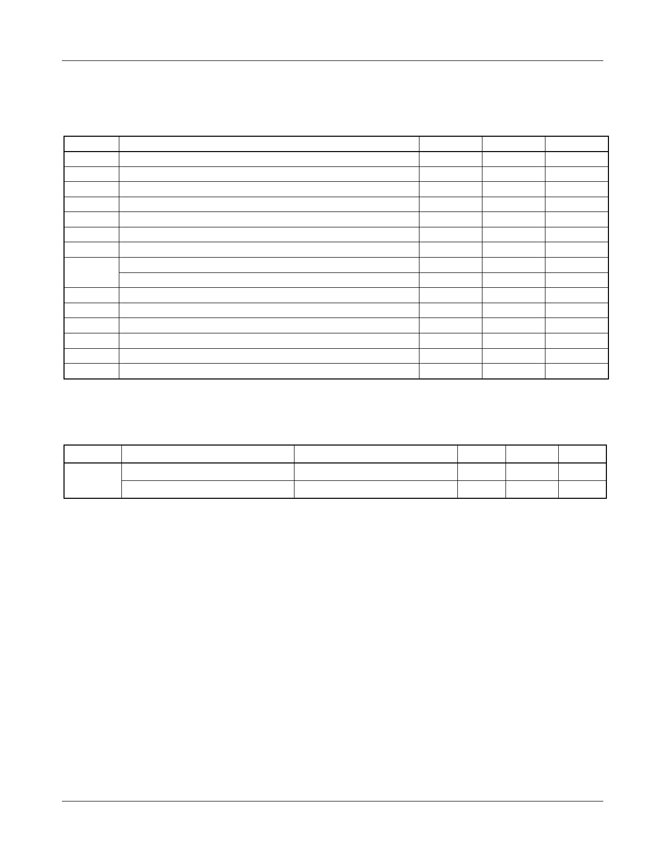
Table 4. A.C. CHARACTERISTICS (VCC = 3.3 V ± 10%, TA = −40°C to +125°C) (Note 3)
Symbol
Parameter
Min
Max
Units
FSCL (Note 4)
tHIGH
tLOW
tTIMEOUT (Note 4)
tR (Note 5)
tF (Note 5)
tSU:DAT (Note 6)
tHD:DAT (Note 5)
Clock Frequency
High Period of SCL Clock
Low Period of SCL Clock
SMBus SCL Clock Low Timeout
SDA and SCL Rise Time
SDA and SCL Fall Time
Data Setup Time
Data Hold Time (for Input Data)
Data Hold Time (for Output Data)
10
400
kHz
600
ns
1300
ns
25
35
ms
300
ns
300
ns
100
ns
0
ns
300
900
ns
tSU:STA
START Condition Setup Time
600
ns
tHD:STA
START Condition Hold Time
600
ns
tSU:STO
STOP Condition Setup Time
600
ns
tBUF
Bus Free Time Between STOP and START
1300
ns
Ti
Noise Pulse Filtered at SCL and SDA Inputs
100
ns
tPU (Note 7)
Power−up Delay to Valid Temperature Recording
100
ms
3. Timing reference points are set at 30%, respectively 70% of VCC, as illustrated in Figure 11. Bus loading must be such as to allow meeting
the VIL, VOL as well as the various timing limits.
4. The TS interface will reset itself and will release the SDA line if the SCL line stays low beyond the tTIMEOUT limit. The time−out count is started
(and then re−started) on every negative transition of SCL in the time interval between START and STOP.
5. In a “Wired−OR” system (such as I2C or SMBus), SDA rise time is determined by bus loading. Since each bus pull−down device must be
able to sink the (external) bus pull−up current (in order to meet the VIL and/or VOL limits), it follows that SDA fall time is inherently faster than
SDA rise time. SDA rise time can exceed the standard recommended tR limit, as long as it does not exceed tLOW − tHD:DAT − tSU:DAT, where
tLOW and tHD:DAT are actual values (rather than spec limits). A shorter tHD:DAT leaves more room for a longer SDA tR, allowing for a more
capacitive bus or a larger bus pull−up resistor. At the minimum tLOW spec limit of 1300 ns, the maximum tHD:DAT of 900 ns demands a
maximum SDA tR of 300 ns. The CAT6095’s maximum tHD:DAT is <700 ns, thus allowing for an SDA tR of up to 500 ns at minimum tLOW.
6. The minimum tSU:DAT of 100 ns is a limit recommended by standards. The TS will accept a tSU:DAT of 0 ns.
7. The first valid temperature recording can be expected after tPU at nominal supply voltage.
Table 5. PIN CAPACITANCE (TA = 25°C, VCC = 3.3 V, f = 1 MHz)
Symbol
Parameter
Test Conditions/Comments
Min
Max
Unit
CIN
SDA, EVENT Pin Capacitance
VIN = 0
8
pF
Input Capacitance (other pins)
VIN = 0
6
pF
http://onsemi.com
3
Share Link: 