IDT72V3660L7.5PF Просмотр технического описания (PDF) - Integrated Device Technology
Номер в каталоге
Компоненты Описание
Список матч
IDT72V3660L7.5PF Datasheet PDF : 36 Pages
| |||
IDT72V3640/50/60/70/80/90/110 3.3V HIGH DENSITY SUPERSYNC IITM 36-BIT FIFO
1,024 x 36, 2,048 x 36, 4,096 x 36, 8,192 x 36, 16,384 x 36, 32,768 x 36, 65,536 x 36, 131,072 x 36
COMMERCIAL AND INDUSTRIAL
TEMPERATURE RANGES
DESCRIPTION:
The IDT72V3640/72V3650/72V3660/72V3670/72V3680/72V3690/
72V36100/72V36110 are exceptionally deep, high speed, CMOS First-In-
First-Out (FIFO) memories with clocked read and write controls and a flexible
Bus-Matching x36/x18/x9 data flow. These FIFOs offer several key user
benefits:
• Flexible x36/x18/x9 Bus-Matching on both read and write ports
• The period required by the retransmit operation is fixed and short.
• Thefirstworddatalatencyperiod,fromthetimethefirstwordiswrittentoan
empty FIFO to the time it can be read, is fixed and short.
• High density offerings up to 4 Mbit
Bus-Matching Sync FIFOs are particularly appropriate for network, video,
telecommunications, data communications and other applications that need to
buffer large amounts of data and match busses of unequal sizes.
Each FIFO has a data input port (Dn) and a data output port (Qn), both of
which can assume either a 36-bit, 18-bit or a 9-bit width as determined by the
state of external control pins Input Width (IW), Output Width (OW), and Bus-
Matching (BM) pin during the Master Reset cycle.
The input port is controlled by a Write Clock (WCLK) input and a Write Enable
(WEN) input. Data is written into the FIFO on every rising edge of WCLK when
WEN is asserted. The output port is controlled by a Read Clock (RCLK) input
and Read Enable (REN) input. Data is read from the FIFO on every rising edge
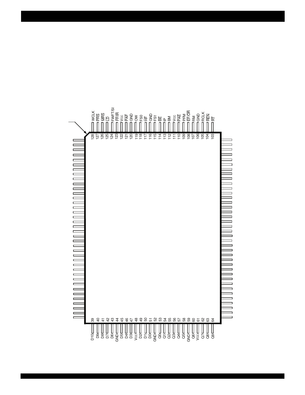
PIN CONFIGURATIONS
INDEX
WEN
1
SEN
2
DNC(1)
3
VCC
4
DNC(1)
5
IW
6
D35
7
D34
8
D33
9
D32
10
VCC
11
D31
12
D30
13
GND
14
D29
15
D28
16
D27
17
D26
18
D25
19
D24
20
D23
21
GND
22
D22
23
VCC
24
D21
25
D20
26
D19
27
D18
28
GND
29
D17
30
D16
31
D15
32
D14
33
D13
34
VCC
35
D12
36
GND
37
D11
38
102
OE
101
VCC
100
VCC
99
Q35
98
Q34
97
Q33
96
Q32
95
GND
94
GND
93
Q31
92
Q30
91
Q29
90
Q28
89
Q27
88
Q26
87
VCC
86
Q25
85
Q24
84
GND
83
GND
82
Q23
81
Q22
80
Q21
79
Q20
78
Q19
77
Q18
76
GND
75
Q17
74
Q16
73
VCC
72
VCC
71
Q15
70
Q14
69
Q13
68
Q12
67
GND
66
Q11
65
Q10
NOTE:
1. DNC = Do Not Connect.
TQFP (PK128-1, order code: PF)
TOP VIEW
2
4667 drw 02
Share Link: 