PI3B16213V Просмотр технического описания (PDF) - Pericom Semiconductor
Номер в каталоге
Компоненты Описание
Список матч
PI3B16213V Datasheet PDF : 4 Pages
| |||
PI3B16213
11223344556677889900112233445566778899001122334455667788990011221122334455667788990011223344556677889900112233445566778899001122112233445566778899001122334455667788990011223344556677889900112231122.33344V55667728849900-11B2233i44t55B6677u8899s00-11E2233x4455c66h7788a9900n11g2211e2233S44w556677it8899c00h1122
Maximum Ratings
(Above which useful life may be impaired. For user guidelines, not tested.)
Storage Temperature .................................................... 65°C to +150°C
Ambient Temperature with Power Applied .................... 40°C to +85°C
Note:
Stresses greater than those listed under MAXIMUM
RATINGS may cause permanent damage to the device. This
Supply Voltage Range ................................................... 0.5Vto+4.60V is a stress rating only and functional operation of the device
DC Input Voltage ........................................................... 0.5Vto+4.60V
DC Output Current ...................................................................... 120mA
at these or any other conditions above those indicated in
the operational sections of this specification is not implied.
Exposure to absolute maximum rating conditions for ex-
Power Dissipation ............................................................................. 1 W tended periods may affect reliability.
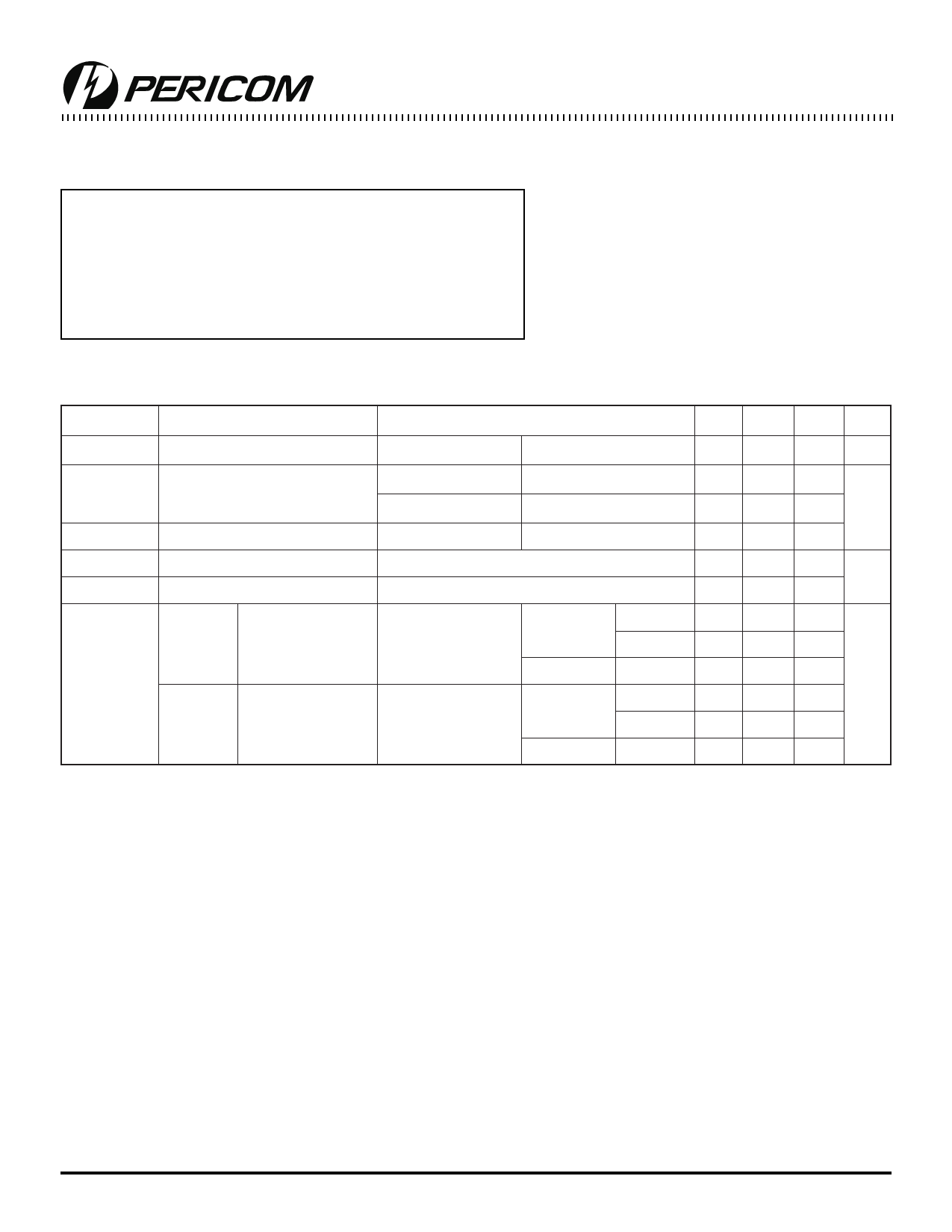
Electrical Characteristics (Over the Operating Range, TA = 40°C to +85°C, VCC = 3.0V to 3.6V)
Parameters
Description
Test Conditions
Min. Typ(1) Max. Units
VIK
II
ICC
CIN(2)
COFF(2)
RON(3)
Input HIGH Voltage
VCC = Min.
II = 18mA
Input Current
VCC = 0
VCC = Max.
VI = Max.
VI = Max. or GND
Quiescent Power Supply Current VCC = Max. IO = 0 VI =VCC or GND
Input Capacitance
VIN = 0V
Switch Off, A/B Capacitance VIN = 0V; S0, S1, S2 = GND
A to B
VCC = Min.
VCC = Min
VI = 0
II = 30mA,
II = 64mA
VI = 2.4 V II = 15mA
A1 to A2 VCC = Min.
VCC = Min
VI = 0
II = 30mA,
II = 64mA
VI = 2.4 V II = 15mA
1.2 V
10
±1 µA
10
3
pF
14
5
8
5
8
10 15
Ω
10 14
10 14
20 30
Notes:
1. Typical values are at VCC = 3.3V, TA = 25°C ambient and maximum loading.
2. This parameter is determined by device characterization but is not production tested.
3. Measured by the voltage drop between A and B pin at indicated current through the switch. ON resistance is determined
by the lower of the voltages on the two (A,B) pins.
2
PS8169A 08/21/01
Share Link: 