PI6C2305-1LI Просмотр технического описания (PDF) - Pericom Semiconductor
Номер в каталоге
Компоненты Описание
Список матч
PI6C2305-1LI Datasheet PDF : 9 Pages
| |||
PI6C2305/PI6C2309 1122334455667788990011223344556677889900112233445566778899001122112233445566778899001122334455667788990011223344556677889900112211223344556677889900112233445566778899001122334455667788990011221122334455667788990011223344556677889900112233445566778899001122112233445566778899001122
Zero-Delay Clock Buffer
Product Features
• Maximum rated frequency: 133 MHz
• Low cycle-to-cycle jitter
• Input to output delay, less than 200ps
• Internal feedback allows outputs to be synchronized
to the clock input
• 5V tolerant input*
• Operates at 3.3V VDD
• Space-saving Packages:
150-mil SOIC (W)
173-mil TSSOP (L)
* FB_IN and CLKIN must reference the same voltage thresh-
olds for the PLL to deliver zero delay skewing
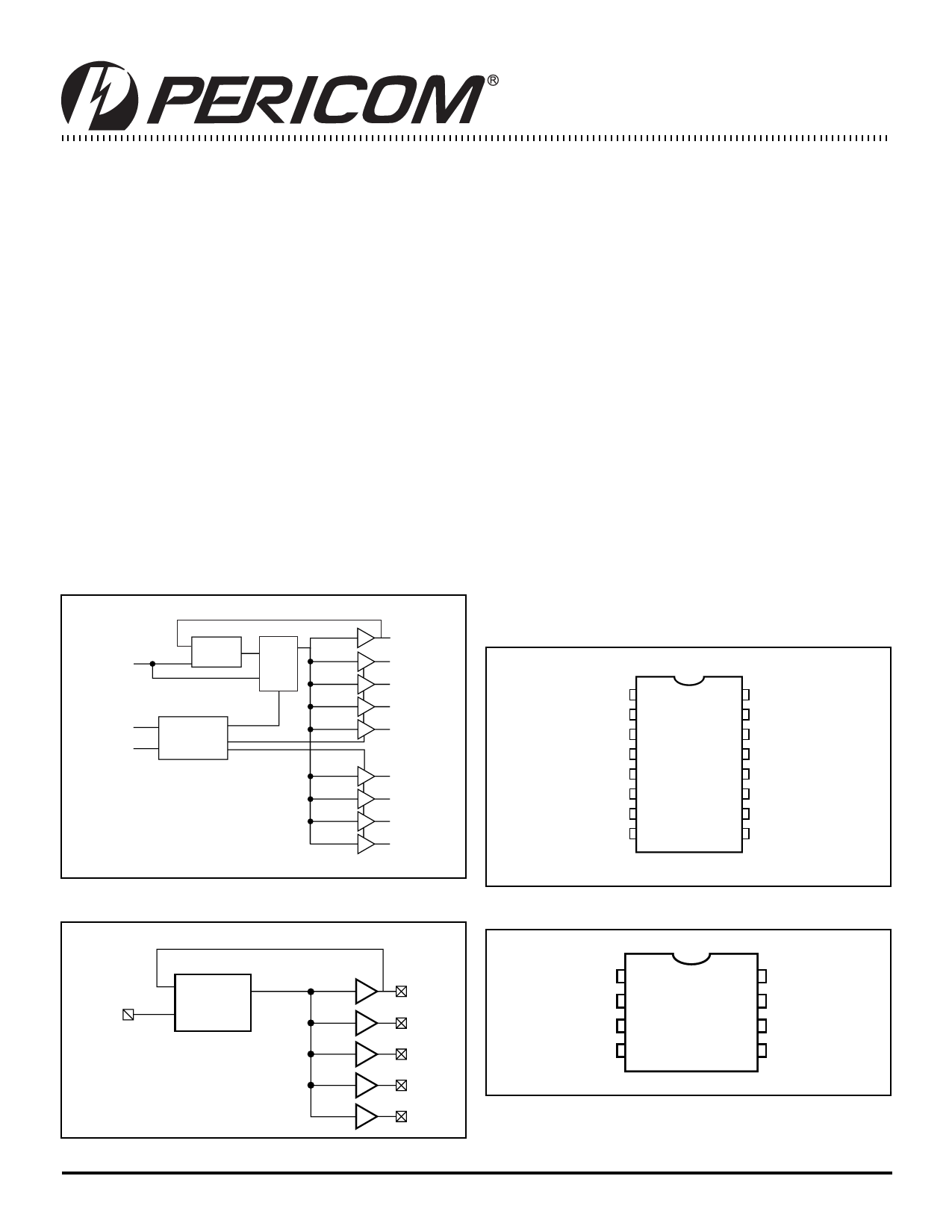
Block Diagram: PI6C2309
CLKIN
PLL
MUX
SEL1
SEL2
Decode
Logic
PI6C2309 (-1, -1H)
OUT0
OUTA1
OUTA2
OUTA3
OUTA4
OUTB1
OUTB2
OUTB3
OUTB4
Functional Description
The PI6C230x is a PLL based, zero-delay buffer, with the ability
to distribute five outputs on PI6C2305, nine outputs on PI6C2309 of
up to 133MHz at 3.3V. All the outputs are distributed from a single
clock input CLKIN and output CLK0 performs zero delay by connect-
ing a feedback to PLL.
PI6C2309 has two banks of four outputs that can be controlled by
the selection inputs, SEL1 & SEL2. It also has a powersparing feature:
when input SEL1 is 0 and SEL2 is 1, PLL is turned off and all
outputs are referenced from CLKIN. PI6C2305 is an 8-pin version
of PI6C2309 without selection inputs. PI6C230X is available in
high drive and industrial environment versions.
An internal feedback on OUT0 is used to synchronize the outputs
to the input; the relationship between loading of this signal
and the outputs determines the input-output delay.
PI6C230X are characterized for both commercial and industrial
operation
Notice: This device is subject to import restriction. Please refer
to the Import Restriction Notice under the Ordering Information
section.
Pin Configuration PI6C2309
CLKIN
OUTA1
OUTA2
VDD
GND
OUTB1
OUTB2
SEL2
1
16
2
15
3
4
5
16-Pin
W, L
14
13
12
6
11
7
10
8
9
OUT0
OUTA4
OUTA3
VDD
GND
OUTB4
OUTB3
SEL1
Block Diagram: PI6C2305
Pin Configuration: PI6C2305
PLL
CLKIN
PI6C2305(–1, –1H)
OUT0
OUT1
OUT2
OUT3
OUT4
CLKIN 1
CLK2 2
CLK1 3
GND 4
8-Pin
W, L
8 CLK0
7 CLK4
6 VDD
5 CLK3
1
PS8478B 10/30/01
Share Link: 