RT9202CS Просмотр технического описания (PDF) - Richtek Technology
Номер в каталоге
Компоненты Описание
Список матч
RT9202CS Datasheet PDF : 16 Pages
| |||
RT9202
Input / Output Capacitor
High frequency/long life decoupling capacitors should
be placed as close to the power pins of the load as
physically possible. Be careful not to add inductance
to the PCB trace, as it could eliminate the
performance from utilizing these low inductance
components. Consult with the manufacturer of the
load on specific decoupling requirements.
The output capacitors are necessary for filtering
output and stabilizing the close loop (see the PWM
loop stability). For powering advanced, high-speed
processors, it is required to meet with the
requirement of fast load transient, high frequency
capacitors with low ESR/ESL capacitors are
recommended.
Another concern is high ESR induced ripple may
trigger UV or OV protections.
PWM Loop Stability
The RT9202 is a voltage mode buck controller
designed for 5V step-down applications. The gain of
error amplifier is fixed at 35dB for simplified design.
The output amplitude of ramp oscillator is 1.6V, the
loop gain and loop pole/zero are calculated as
follows:
DC loop gain GA = 35dB ×
LC
filter
pole
PO
=
1
2
×
π
×
5×
1.6
LC
0.8
VOUT
Error Amp pole PA = 300kHz
ESR zero ZO =
1 × π × ESR × C
2
The RT9202 Bode plot as shown Fig.6 is stable in
most of application conditions.
VOUT = 3.3V
COUT = 1500µF(33mΩ)
L=2µH
40 VOUT = 1.5V
VOUT = 2.5V
30 VOUT = 3.3V
PO = 2.9kHz
ZO = 3.2kHz
20
Loop Gain
10
100
1k
10k
100k
1M
Fig. 6
www.richtek.com
12
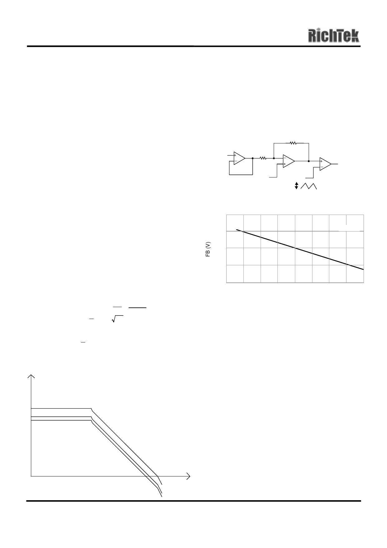
Reference Voltage
Because RT9202 use a low 35dB gain error amplifier,
shown in Fig. 7. The voltage regulation is dependent
on VIN & VOUT setting. The FB reference voltage of
0.8V were trimmed at VIN = 5V & VOUT = 2.5V
condition. In a fixed VIN = 5V application, the FB
reference voltage vs. VOUT voltage can be calculated
as Fig. 8.
I3
56K
FB
I2
1K
EA
PWM
REP
0.8V
RAMP
1.75V
Fig. 7
0.82
0.81
VIN = 5V
0.80
0.79
0.78
0.5
1 1.5
2
2.5 3
3.5 4 4.5
VOUT (V)
Fig. 8
Feedback Divider
The reference of RT9202 is 0.8V. The output voltage
can be set using a resistor based divider as shown in
Fig.9. Put the R1 and R2 as close as possible to FB
pin and R2 should less than 1 kΩ to avoid noise
coupling. The C1 capacitor is a speed-up capacitor
for reducing output ripple to meet with the
requirement of fast transient load. Typically a 1nF ~
0.1µF is enough for C1.
DS9202-02 August 2002
Share Link: 