MAX710C/D Просмотр технического описания (PDF) - Maxim Integrated
Номер в каталоге
Компоненты Описание
Список матч
MAX710C/D Datasheet PDF : 12 Pages
| |||
MAX710/MAX711
3.3V/5V or Adjustable,
Step-Up/Down DC-DC Converters
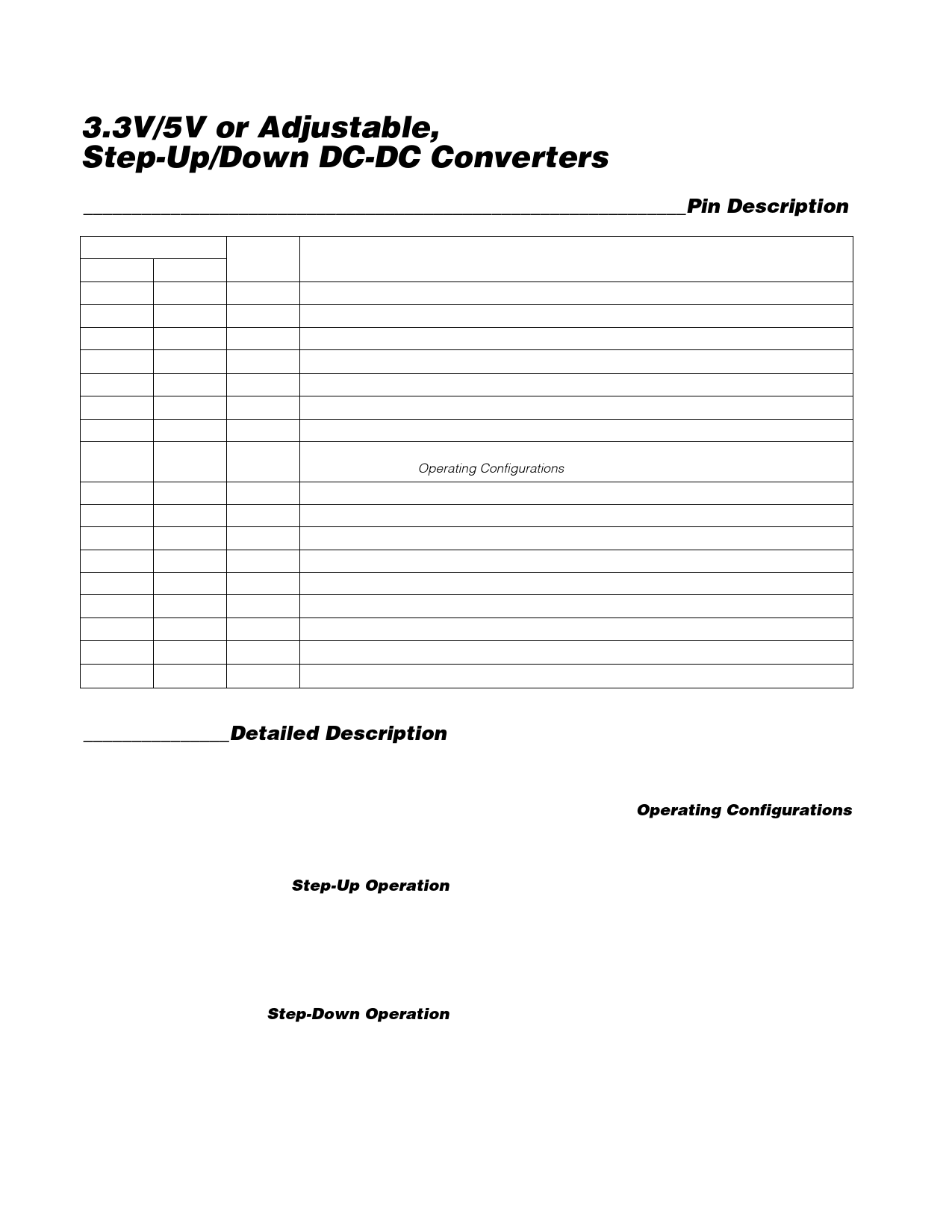
______________________________________________________________Pin Description
PIN
MAX710 MAX711
1
1
2
2
3
3
4
4
5
5
6
—
—
6
7
7
8
8
9
9
10
10
11
11
12
12
13
13
14
14
15
15
16
16
NAME
LX
PGND
ILIM
SHDN
STBY
3/5
FB
N/E
LBO
OUT
LBI-
LBI+
PS
REF
GND
PGND
LX
FUNCTION
Drain Connection for internal N-channel power MOSFET
Power Ground
Inductor Current-Limit-Select Input. Connect to GND for 1.5A limit and to PS for 0.8A limit.
Shutdown Input. When low, the entire circuit is off and OUT is actively pulled to GND.
Standby Input. Connect to GND to disable boost circuit. Connect to PS for normal operation.
Selects the output voltage. Connect to GND for 5V output and to OUT for 3.3V output.
Feedback Input
Selects low-noise or high-efficiency mode. Connect to GND for high efficiency and to PS for
lowest noise. See Operating Configurations section.
Low-Battery Comparator Output
Linear-Regulator Output. Bypass with a 4.7µF capacitor to GND.
Negative Input to Low-Battery Comparator
Positive Input to Low-Battery Comparator
Source of internal PFET regulator. The IC is powered from PS.
1.28V Reference Voltage Output. Bypass with a 0.1µF capacitor to GND.
Analog Ground. Must be low impedance. Solder directly to ground plane.
Power Ground
Drain Connection for internal N-channel power MOSFET
_______________Detailed Description
The MAX710/MAX711 integrate a step-up DC-DC con-
verter with a linear regulator to provide step-up/down
voltage conversion. The step-up switch-mode regulator
contains an N-channel power MOSFET switch. It also
shares a precision voltage reference with a linear regu-
lator that contains a P-channel MOSFET pass element
(Figure 1).
Step-Up Operation
A pulse-frequency-modulation (PFM) control scheme
with a constant 1µs off-time and variable on-time con-
trols the N-channel MOSFET switch. The N-channel
switch turns off when the part reaches the peak current
limit or the 4µs maximum on-time. The ripple frequency
is a function of load current and input voltage.
Step-Down Operation
The low-dropout linear regulator consists of a refer-
ence, an error amplifier, and a P-channel MOSFET. The
reference is connected to the error amplifier’s inverting
input. The error amplifier compares this reference with
the selected feedback voltage and amplifies the differ-
ence. The difference is conditioned and applied to the
P-channel pass transistor’s gate.
Operating Configurations
The MAX710/MAX711 have several operating configu-
rations to minimize noise and optimize efficiency for dif-
ferent input voltage ranges. These configurations are
accomplished via the N/E input, which controls opera-
tion of the on-chip linear regulator.
With N/E low, the linear regulator behaves as a 0.7Ω (at
5V output) PFET switch when the IC is boosting, and as
a conventional linear regulator when VIN > VOUT. This
provides optimum boost efficiency, but the PFET does
little to reject boost-converter output ripple. With N/E
high, boost ripple rejection is optimized by maintaining
headroom (VFV, typically 0.5V at 5V output) across the
linear regulator. Boost mode efficiency is then about
10% lower than with N/E high.
6
Maxim Integrated
Share Link: 