74LVT16501ADL(2006) Просмотр технического описания (PDF) - Philips Electronics
Номер в каталоге
Компоненты Описание
Список матч
74LVT16501ADL Datasheet PDF : 19 Pages
| |||
Philips Semiconductors
74LVT16501A
3.3 V LVT 18-bit universal bus transceiver; 3-state
Table 7. Static characteristics …continued
At recommended operating conditions; voltages are referenced to GND (ground = 0 V).
Symbol Parameter
Conditions
Min Typ Max Unit
∆ICC
Ci
additional quiescent supply
current
per input pin; VCC = 3.0 V to 3.6 V;
[7] -
one input at VCC − 0.6 V, other inputs
at VCC or GND
input capacitance (control pins) VI = 0 V or 3.0 V
-
0.1 0.2 mA
3
-
pF
Cio
input/output capacitance
(I/O pins)
outputs disabled; VI/O = 0 V or 3.0 V
-
9
-
pF
[1] Typical values are at VCC = 3.3 V and Tamb = 25 °C.
[2] For valid test results, data must not be loaded into the flip-flops (or latches) after applying power.
[3] Unused pins at VCC or GND.
[4] This is the bus hold overdrive current required to force the input to the opposite logic state.
[5] This parameter is valid for any VCC between 0 V and 1.2 V with a transition time of up to 10 ms. From VCC = 1.2 V to VCC = 3.3 V ± 0.3 V
a transition time of 100 µs is permitted. This parameter is valid for Tamb = 25 °C only.
[6] ICC is measured with outputs pulled to VCC or GND.
[7] This is the increase in supply current for each input at the specified voltage level other than VCC or GND.
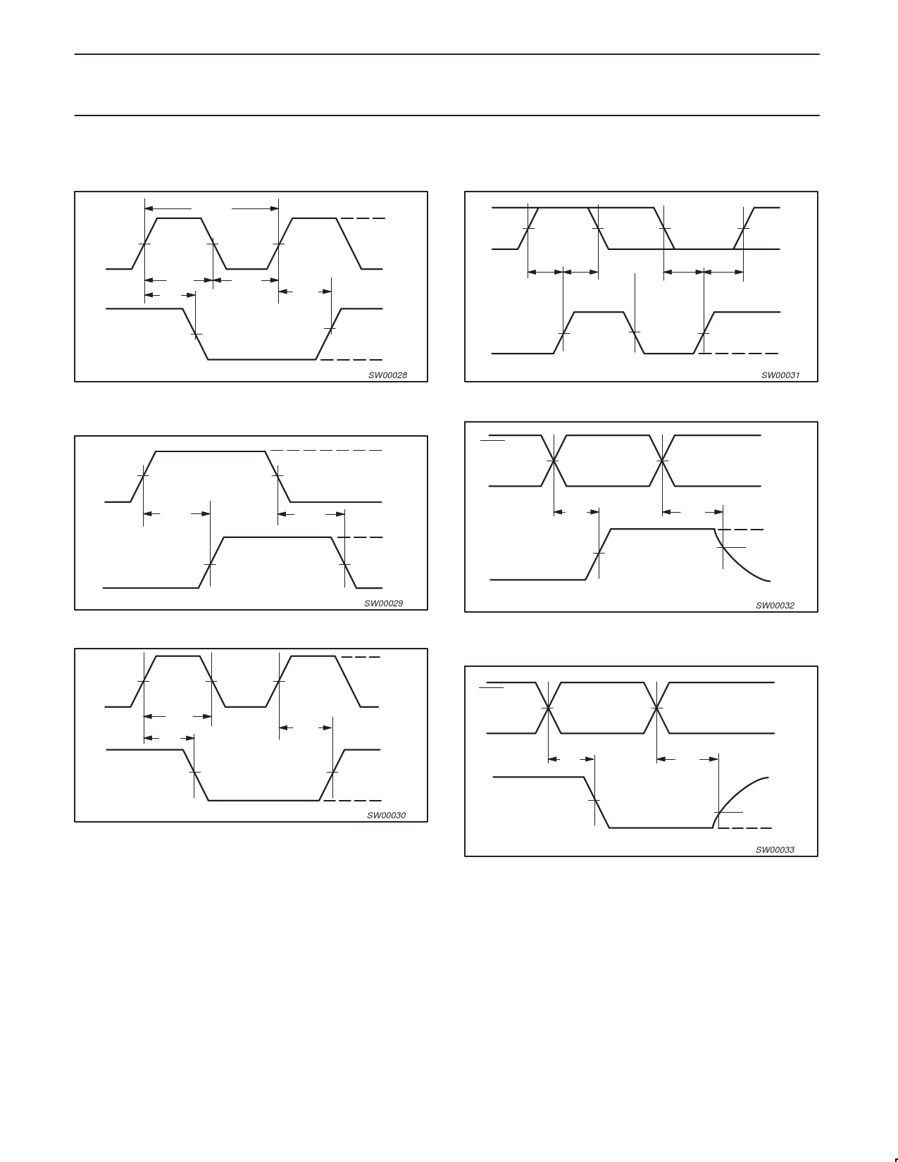
11. Dynamic characteristics
Table 8. Dynamic characteristics
Voltages are referenced to GND (ground = 0 V); for test circuit see Figure 11.
Symbol Parameter
Conditions
VCC = 2.7 V; Tamb = −40 °C to +85 °C
tPLH
propagation delay
An to Bn or Bn to An
see Figure 5
CPAB to Bn or CPBA to An
see Figure 6
LEAB to Bn or LEBA to An
see Figure 7
tPHL
propagation delay
An to Bn or Bn to An
see Figure 5
CPAB to Bn or CPBA to An
see Figure 6
LEAB to Bn or LEBA to An
see Figure 7
tPZH
tPZL
tPHZ
tPLZ
tsu(H)
output enable time to HIGH-state
output enable time to LOW-state
output disable time from HIGH-state
output disable time from LOW-state
setup time HIGH
An to CPAB or Bn to CPBA
see Figure 8
see Figure 9
see Figure 8
see Figure 9
see Figure 10
An to LEAB with CPAB LOW or
Bn to LEBA with CPBA LOW
An to LEAB with CPAB HIGH or
Bn to LEBA with CPBA HIGH
Min Typ Max Unit
-
-
-
-
-
-
-
-
-
-
-
-
-
-
-
-
-
-
-
-
-
-
2.4 -
2.0 -
1.5 -
5.4 ns
6.4 ns
6.4 ns
5.4 ns
6.4 ns
6.4 ns
5.5 ns
5.2 ns
6.3 ns
5.6 ns
-
ns
-
ns
-
ns
74LVT16501A_4
Product data sheet
Rev. 04 — 19 May 2006
© Koninklijke Philips Electronics N.V. 2006. All rights reserved.
9 of 19
Share Link: 