IDT74FCT163244CPF Просмотр технического описания (PDF) - Integrated Device Technology
Номер в каталоге
Компоненты Описание
Список матч
IDT74FCT163244CPF Datasheet PDF : 6 Pages
| |||
IDT74FCT163244/A/C
3.3V 16-BIT BUFFER/LINE DRIVER
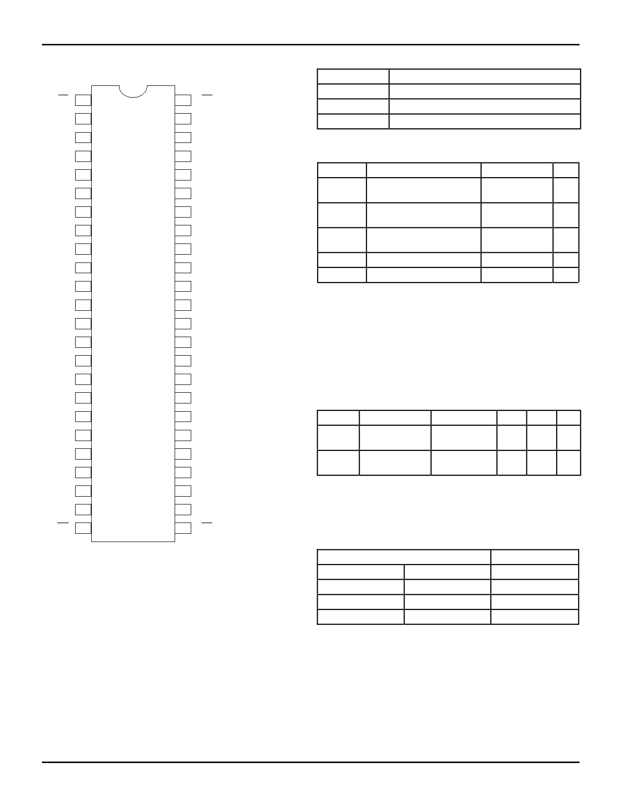
PIN CONFIGURATIONS
1OE
1Y1
1Y2
GND
1Y3
1Y4
VCC
2Y1
2Y2
GND
2Y3
2Y4
3Y1
3Y2
GND
3Y3
3Y4
VCC
4Y1
4Y2
GND
4Y3
4Y4
4OE
1
48
2
47
3
46
4
45
5
44
6
43
7
42
8
41
9
40
10
39
11
38
12 SO48-1 37
SO48-2
13 SO48-3 36
14
35
15
34
16
33
17
32
18
31
19
30
20
29
21
28
22
27
23
26
24
25
SSOP/
TSSOP/TVSOP
TOP VIEW
2OE
1A1
1A2
GND
1A3
1A4
VCC
2A1
2A2
GND
2A3
2A4
3A1
3A2
GND
3A3
3A4
VCC
4A1
4A2
GND
4A3
4A4
3OE
2532 drw 03
COMMERCIAL TEMPERATURE RANGES
PIN DESCRIPTION
Pin Names
Description
xOE
3–State Output Enable Inputs (Active LOW)
xAx
Data Inputs
xYx
3-State Outputs
2532 tbl 01
ABSOLUTE MAXIMUM RATINGS(1)
Symbol
VTERM(2)
VTERM(3)
VTERM(4)
TSTG
Description
Terminal Voltage with
Respect to GND
Terminal Voltage with
Respect to GND
Terminal Voltage with
Respect to GND
Storage Temperature
Max.
Unit
–0.5 to +4.6 V
–0.5 to +7.0 V
–0.5 to
V
VCC + 0.5
–65 to +150 °C
IOUT
DC Output Current
–60 to +60 mA
NOTES:
2532 lnk 03
1. Stresses greater than those listed under ABSOLUTE MAXIMUM RAT-
INGS may cause permanent damage to the device. This is a stress rating
only and functional operation of the device at these or any other conditions
above those indicated in the operational sections of this specification is
not implied. Exposure to absolute maximum rating conditions for ex-
tended periods may affect reliability.
2. Vcc terminals.
3. Input terminals.
4. Output and I/O terminals.
CAPACITANCE (TA = +25°C, f = 1.0MHz)
Symbol Parameter(1) Conditions Typ. Max. Unit
CIN
Input
VIN = 0V
3.5 6.0 pF
Capacitance
COUT Output
VOUT = 0V 3.5 8.0 pF
Capacitance
NOTE:
2532 lnk 04
1. This parameter is measured at characterization but not tested.
FUNCTION TABLE(1)
Inputs
xOE
L
L
H
NOTE:
1. H = HIGH Voltage Level
L = LOW Voltage Level
X = Don’t Care
Z = High Impedance
xAx
L
H
X
Outputs
xYx
L
H
Z
2532 tbl 02
8.1
2
Share Link: 