IDT74FCT163344A(2004) Просмотр технического описания (PDF) - Integrated Device Technology
Номер в каталоге
Компоненты Описание
Список матч
IDT74FCT163344A Datasheet PDF : 7 Pages
| |||
IDT74FCT163344A/C
3.3V CMOS ONE-TO-FOUR ADDRESS/CLOCK DRIVER
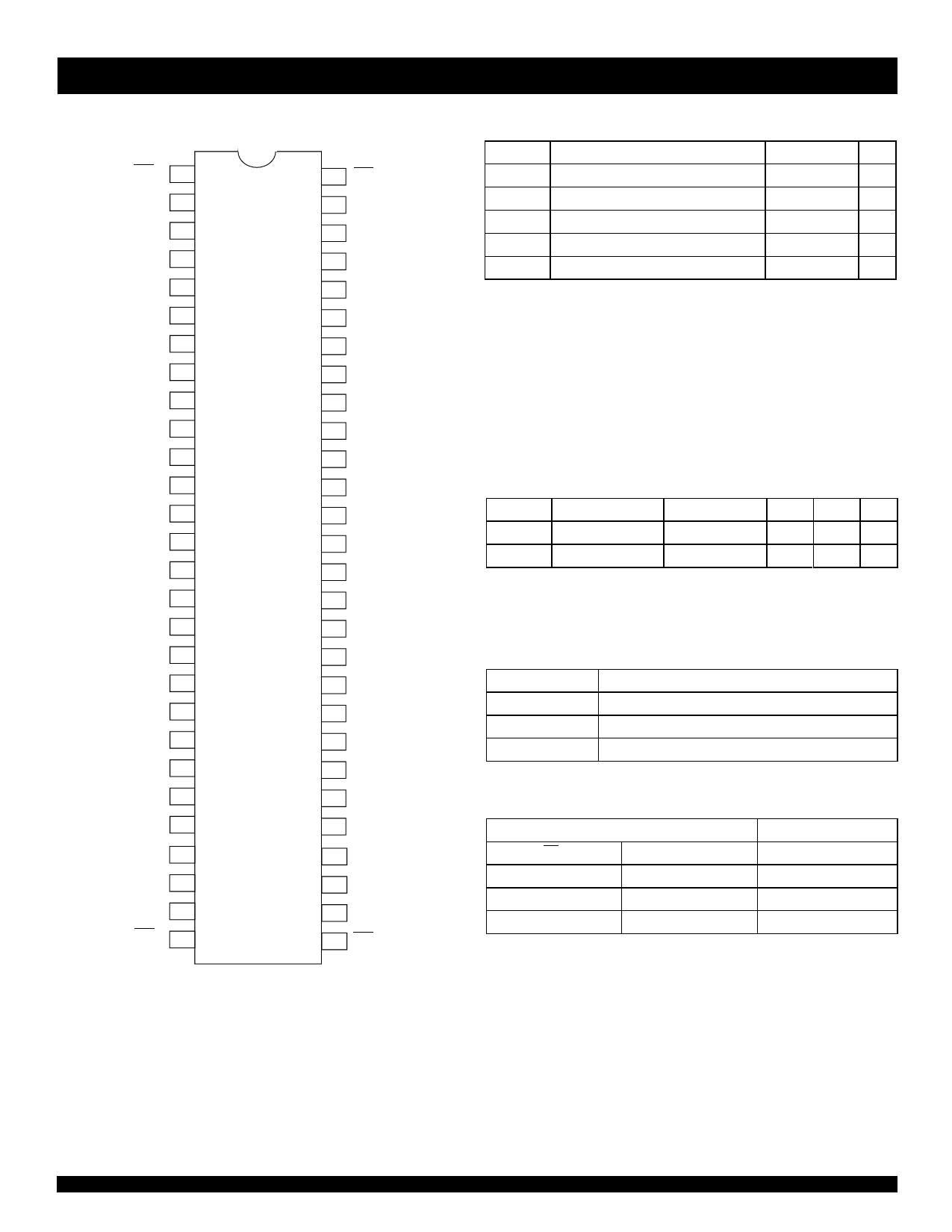
PIN CONFIGURATION
OE1
1
B11
2
B12
3
GND
4
B13
5
B14
6
VCC
7
A1
8
B21
9
B22
10
GND
11
B23
12
B24
13
A2
14
A3
15
B31
16
B32
17
GND
18
B33
19
B34
20
A4
21
VCC
22
B41
23
B42
24
GND
25
B43
26
B44
27
OE2
28
56 OE4
55
B81
54
B82
53 GND
52
B83
51
B84
50
VCC
49 A8
48
B71
47
B72
46 GND
45
B73
44
B74
43
A7
42
A6
41
B61
40
B62
39 GND
38
B63
37
B64
36
A5
35
VCC
34
B51
33
B52
32
GND
31
B53
30
B54
29
OE3
SSOP/ TSSOP
TOP VIEW
INDUSTRIAL TEMPERATURE RANGE
ABSOLUTE MAXIMUM RATINGS(1)
Symbol
Description
Max
Unit
VTERM(2) Terminal Voltage with Respect to GND –0.5 to +4.6
V
VTERM(3) Terminal Voltage with Respect to GND
–0.5 to 7
V
VTERM(4) Terminal Voltage with Respect to GND –0.5 to VCC+0.5 V
TSTG Storage Temperature
–65 to +150
°C
IOUT
DC Output Current
–60 to +60
mA
NOTES:
1. Stresses greater than those listed under ABSOLUTE MAXIMUM RATINGS may cause
permanent damage to the device. This is a stress rating only and functional operation
of the device at these or any other conditions above those indicated in the operational
sections of this specification is not implied. Exposure to absolute maximum rating
conditions for extended periods may affect reliability.
2. Vcc terminals.
3. Input terminals.
4. Outputs and I/O terminals.
CAPACITANCE (TA = +25°C, F = 1.0MHz)
Symbol
Parameter(1)
Conditions Typ. Max. Unit
CIN
Input Capacitance
VIN = 0V
3.5
6
pF
COUT
Output Capacitance VOUT = 0V 3.5
7
pF
NOTE:
1. This parameter is measured at characterization but not tested.
PIN DESCRIPTION
Pin Names
Description
OEx
3-State Output Enable Inputs (Active LOW)
Ax
Inputs
Bxx
3-State Outputs
FUNCTION TABLE(1)
Inputs
OEx
Ax
L
L
L
H
H
X
NOTE:
1. H = HIGH Voltage Level
L = LOW Voltage Level
X = Don't Care
Z = High-impedance
Outputs
Bxx
L
H
Z
2
Share Link: 