PI74ALVCH16820A Просмотр технического описания (PDF) - Pericom Semiconductor
Номер в каталоге
Компоненты Описание
Список матч
PI74ALVCH16820A Datasheet PDF : 4 Pages
| |||
PI74ALVCH16820 111222333444555666777888999000111222333444555666777888999000111222333444555666777888999000111222111222333444555666777888999000111222333444555666777888999000111222333444555666777888999000111222111222333444555666777888999000111222333444555666777888999000111222333444555666777888999000111222111222333444555666777888999000111222333444555666777888999000111222333444555666777888999000111222111222333444555666777888999000111222
3.3V 10-Bit Flip-Flop with Dual Outputs
and 3-State Outputs
Product Features
PI74ALVCH16820 is designed for low-voltage operation
VCC = 2.3V to 3.6V
Hysteresis on all inputs
Typical VOLP (Output Ground Bounce) < 0.8V
at VCC = 3.3V, TA = 25°C
Typical VOHV (Output VOH Undershoot) < 2.0V
at VCC = 3.3V, TA = 25°C
Bus Hold retains last active bus state during 3-state
eliminating the need for external pullup resistors
Industrial operation: 40°C to +85°C
Packages available:
56-pin 240 mil wide plastic TSSOP (A)
56-pin 300 mil wide plastic SSOP (V)
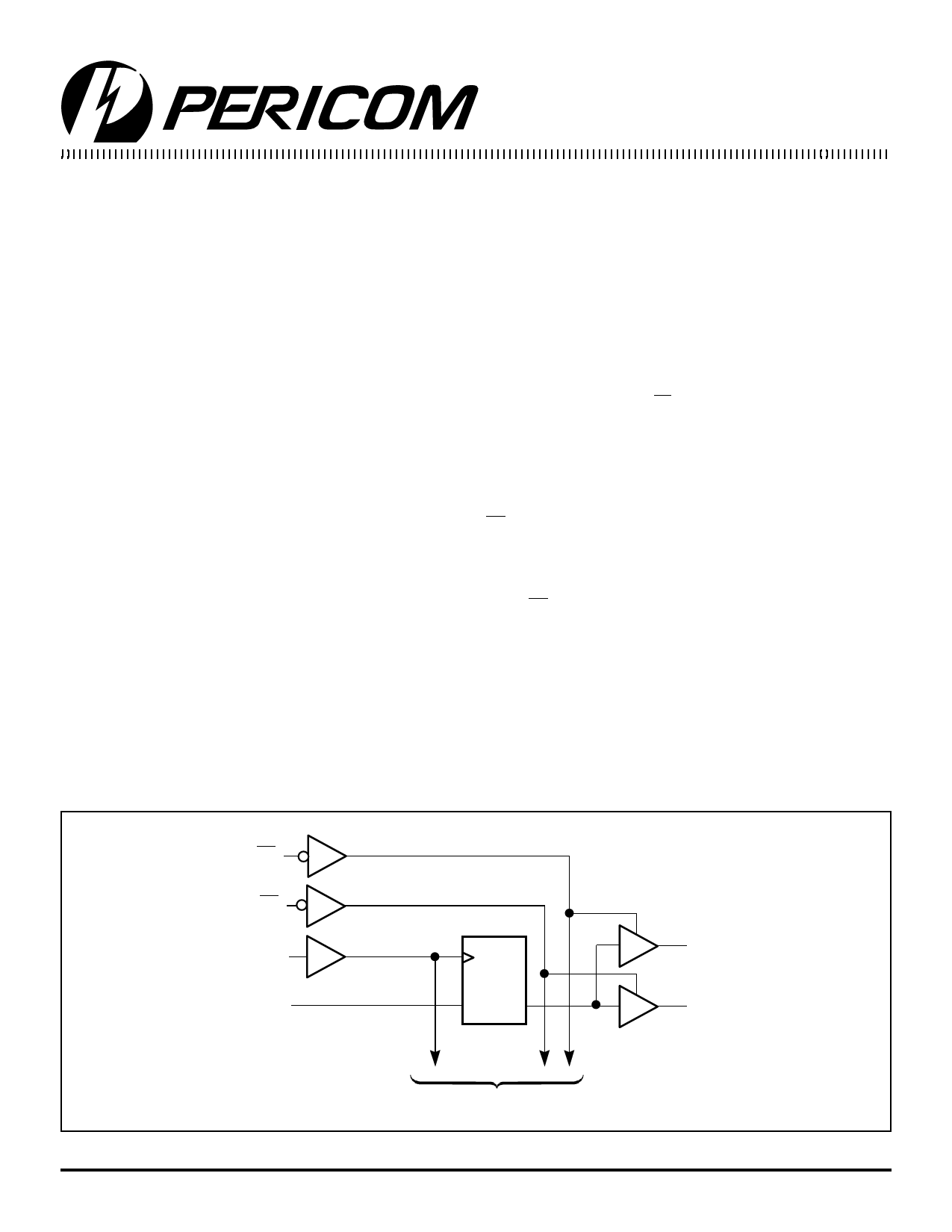
Logic Block Diagram
Product Description
Pericom Semiconductors PI74ALVCH series of logic circuits are
produced using the Companys advanced 0.5 micron CMOS
technology, achieving industry leading speed.
The PI74ALVCH16820, a 10-bit flip-flop designed for 2.3V to 3.3V
VCC operation, features edge-triggered D-type flip-flops. On the
positive transition of clock (CLK) input, the device provides true
data at the Q outputs.
A buffered output-enable (OE) input can be used to place the ten
outputs in either a normal logic state (HIGH or LOW level) or a high-
impedance state. In high-impedance state, outputs neither load nor
drive the bus lines significantly. The high-impedance state and
increased drive are able to drive bus lines without interface or pullup
components.
OE does not affect the internal operation of the flip-flops. Old data
can be retained or new data can be entered while the outputs are in
the high-impedance state.
To ensure the high-impedance state during power up or power
down, OE should be tied to VCC through a pullup resistor whose
minimum value is determined by the current sinking capability of the
driver.
To prevent floating inputs and to eliminate the need for pullup/
down resistors, the PI74ALVCH16820 has Bus Hold which retains
the data inputs last state whenever the data input goes to high-
impedance .
Active bus-hold circuitry is provided to hold unused or floating
data inputs at a valid logic level.
1
1OE
28
2OE
CLK
56
55
D1
C1
1D
2
1Q1
3
1Q2
TO 9 OTHER CHANNELS
1
PS8126A 05/07/01
Share Link: 