RS5C338A-E2 Просмотр технического описания (PDF) - RICOH Co.,Ltd.
Номер в каталоге
Компоненты Описание
Список матч
RS5C338A-E2
RICOH Co.,Ltd.

RS5C338A-E2 Datasheet PDF : 52 Pages
| |||
R×5C338A
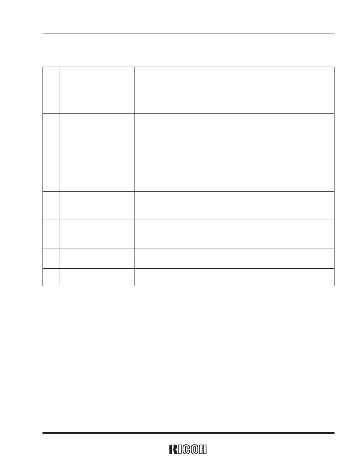
PIN DESCRIPTIONS
Pin No. Symbol
Name
4
CE Chip Enable Input
Description
The CE pin is used for interfacing with the CPU. Should be held high to allow
access to the CPU. Incorporates a pull-down resistor. Should be held low or open
when the CPU is powered off. Allows a maximum input voltage of 5.5 volts regard-
less of supply voltage.
The SCLK pin is used to input clock pulses synchronizing the input and output of
2 SCLK Serial Clock Input data to and from the SIO pin. Allows a maximum input voltage of 5.5 volts regard-
less of supply voltage.
The SIO pin is used to input and output data intended for writing and reading in
3
SIO Serial Input/Output
synchronization with the SCLK pin. CMOS input/output.
The INTR pin is used to output periodic interrupt signals to the CPU and alarm
6 INTR Interrupt Output interrupt signals (Alarm_W, Alarm_D). Disabled at power-on from 0 volts.
Nch. open drain output.
The 32KOUT pin is used to output 32.768-kHz clock pulses. Enabled at power-on
1 32KOUT 32-kHz Clock Output from 0 volts. CMOS output. This pin is disabled if the CLKC pin is set to low or
open.
The CLCK pin is used to control output of the 32KOUT pin. The clock output is
7 CLKC Clock Control Input disabled and held low when the pin is set to low or open. Incorporates a pull-down
resistor.
9 OSCIN Oscillation Circuit The OSCIN and OSCOUT pins are used to connect the 32.768-kHz crystal oscilla-
8 OSCOUT Input/Output
tor (with all other oscillation circuit components built into the R×5C338A.)
10 VDD Positive Power Supply Input
The VDD pin is connected to the power supply. The VSS pin is grounded.
5
VSS Negative Power Supply Input
3
Share Link: