RX5C338A Просмотр технического описания (PDF) - RICOH Co.,Ltd.
Номер в каталоге
Компоненты Описание
Список матч
RX5C338A Datasheet PDF : 52 Pages
| |||
R×5C338A
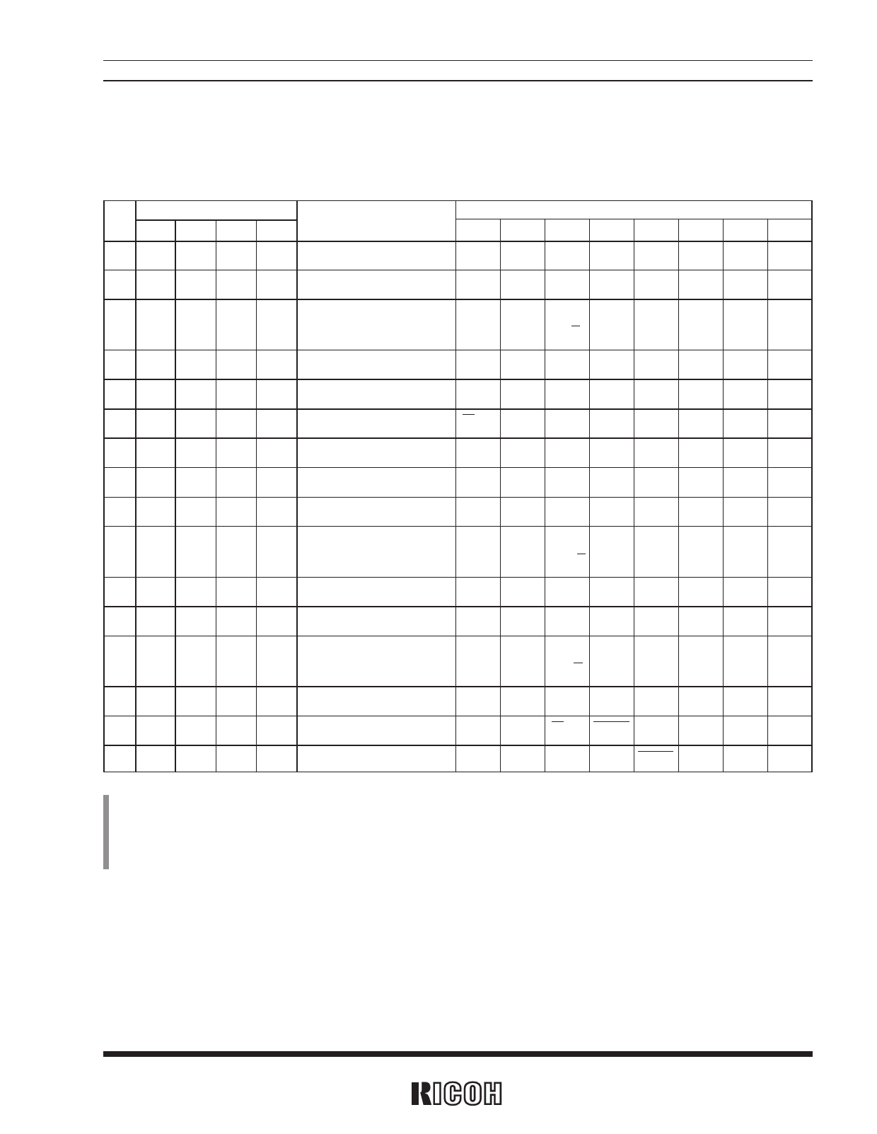
FUNCTIONAL DESCRIPTIONS
1. Address Mapping
Address
A3
A2
A1
A0
Register
00
0
0
0 Second Counter
Data*1
D7 D6 D5 D4 D3 D2 D1 D0
–*2
S40
S20
S10
S8
S4
S2
S1
10
0
0
1 Minute Counter
–
M40 M20 M10 M8
M4
M2
M1
20
0
1
0 Hour Counter
H20
–
–
P/A H10
H8
H4
H2
H1
30
0
1
1 Day-of-week Counter
–
–
–
–
–
W4 W2 W1
40
1
0
0 Day-of-month Counter
–
–
D20 D10 D8
D4
D2
D1
50
1
0
1 Month Counter and Century Bit 19/20 –
– MO10 MO8 MO4 MO2 MO1
60
1
1
0 Year Counter
Y80 Y40
Y20
Y10
Y8
Y4
Y2
Y1
70
1
1
1 Oscillation Adjustment Register*3 (0)*4 F6 F5
F4
F3
F2
F1
F0
81
0
0
0 Alarm_W (minute register) – WM40 WM20 WM10 WM8 WM4 WM2 WM1
WH20
91
0
0
1 Alarm_W (hour register) –
–
WH10 WH8 WH4 WH2 WH1
WP/A
A1
0
1
0 Alarm_W (day-of-week register) – WW6 WW5 WW4 WW3 WW2 WW1 WW0
B1
0
1
1 Alarm_D (minute register) – DM40 DM20 DM10 DM8 DM4 DM2 DM1
DH20
C1
1
0
0 Alarm_D (hour register) –
– DP/A DH10 DH8 DH4 DH2 DH1
D1
1
0
1
–
–
–
–
–
–
–
–
E1
1
1
0 Control Register 1*3
WALE DALE 12/24 CLEN2 TEST CT2 CT1 CT0
F1
1
1
1 Control Register 2*3
VDSL VDET SCRATCH XSTP CLEN1 CTFG WAFG DAFG
*1) All the data listed above accept both reading and writing.
*2) The data marked with “–” is invalid for writing and reset to 0 for reading.
*3) When the XSTP bit is set to 1 in control register 2, all the bits are reset to 0 in oscillation adjustment register 1, control register 1 and control register 2
excluding the XSTP bit.
*4) Writing to the oscillation adjustment register requires zero filling the (0) bit.
9
Share Link: 