MB40958 Просмотр технического описания (PDF) - Fujitsu
Номер в каталоге
Компоненты Описание
Список матч
MB40958 Datasheet PDF : 11 Pages
| |||
MB40958
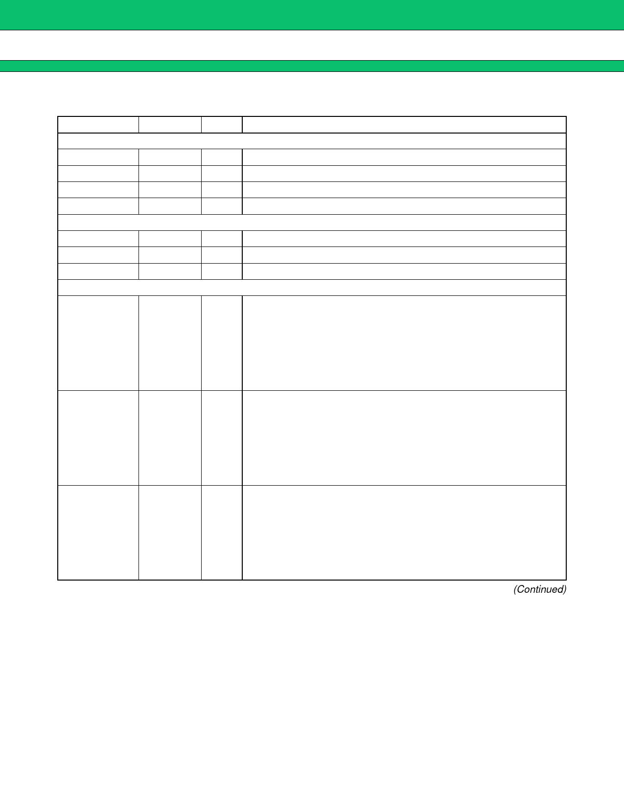
s PIN DESCRIPTION
Symbol
Power Supply
VCCD
D. GND
VCCA
A. GND
Clock
CLKR
CLKG
CLKB
Digital Input
R1
R2
R3
R4
R5
R6
R7
R8
G1
G2
G3
G4
G5
G6
G7
G8
B1
B2
B3
B4
B5
B6
B7
B8
Pin No.
34
48
41, 44, 47
39, 42, 45
1
2
3
4
5
6
7
8
9
10
11
14
15
16
17
18
19
20
21
24
25
26
27
28
29
30
31
Type
Name & Function
— +5V DC power supply pins for digital block.
— Ground pin for digital block.
— DC power supply pins for analog block.
— Ground pins for analog block.
I Clock input pin for R channel.
I Clock input pin for G channel.
I Clock input pin for B channel.
Digital data input pins for R channel.
I 8-bit data is input to the pins.
The R1 pin is the MSB and the R8 pin is the LSB.
Digital data input pins for G channel.
I 8-bit data is input to the pins.
The G1 pin is the MSB and the G8 pin is the LSB.
Digital data input pins for B channel.
I 8-bit data is input to the pins.
The B1 pin is the MSB and the B8 pin is the LSB.
(Continued)
3
Share Link: 