AIC1628 Просмотр технического описания (PDF) - Analog Intergrations
Номер в каталоге
Компоненты Описание
Список матч
AIC1628 Datasheet PDF : 7 Pages
| |||
AIC1628
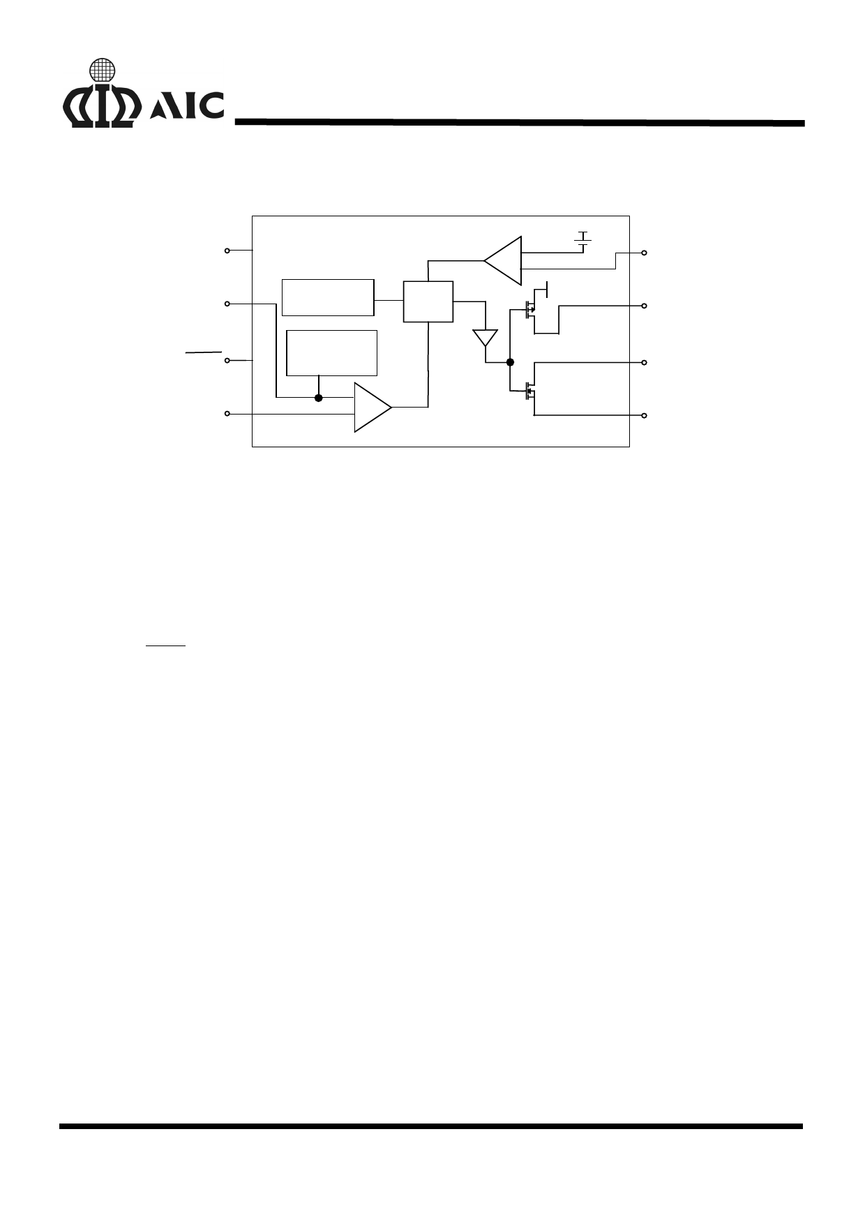
BLOCK DIAGRAM
1
VIN
VREF 2
SHDN 3
FB 4
PFM
OSCILLATOR
1.22V
REFERENCE
VOLTAGE
+
-
CURRENT LIMIT
COMPARATOR
+
-
LATCH
VIN
60mV
VIN
8
CL
7
DHI
OUTPUT DRIVER
6
DLOW
ERROR COMPARATOR
5
GND
PIN DESCRIPTIONS
PIN 1: VIN - 4V to 24V input supply voltage.
PIN 2: VREF - 1.22V reference output. Bypass
with a 0.047µF capacitor to GND.
Sourcing capability is guaran-
teed to be greater than 250µA.
PIN 3:
SHDN - Logical input to shutdown the
chip.
>1.5V = normal operation,
GND = Shutdown,
Can not be floating or forced
greater than 15V. In shutdown
mode DLOW and DHI pins are
at low level.
PIN 4: FB-
Feedback signal input to sense
VREF. Connecting a resistance
R1 to VOUT and a resistance R2
to GND yields the output voltage:
VOUT = (R1+R2)/R2 x VREF
(Refer to typical application cir-
cuit)
PIN 5: GND - Power ground.
PIN 6: DLOW -Driver sinking output. Connected to
gate of the external N-channel MOS-
FET or base of the NPN bipolar tran-
sistor.
PIN 7: DHI
- Driver sourcing output. Connected to
DLOW when using an external N-
channel MOSFET. When using an
external NPN bipolar transistor, con-
nect a base resistance RB from this
pin to DLOW. RB value depends on
VIN, inductor and NPN current gain.
PIN 8: CL
- Current-limit input. Threshold voltage
is 60mV from VIN. This pin clamps
the switch peak current to prevent
over-current damage to the external
switch, under abnormal conditions.
4
Share Link: 