MAX618EEE(1999) Просмотр технического описания (PDF) - Maxim Integrated
Номер в каталоге
Компоненты Описание
Список матч
MAX618EEE Datasheet PDF : 14 Pages
| |||
28V, PWM, Step-Up DC-DC Converter
ABSOLUTE MAXIMUM RATINGS
IN to GND ...............................................................-0.3V to +30V
LX to GND ..............................................................-0.3V to +30V
VL to GND ................................................................-0.3V to +6V
SHDN, COMP, FB to GND ............................-0.3V to (VL + 0.3V)
PGND to GND.....................................................................±0.3V
Continuous Power Dissipation (TA = +70°C) (Note 1)
16-Pin QSOP (derate 15mW/°C above +70°C)...................1W
Operating Temperature Range ...........................-40°C to +85°C
Junction Temperature ......................................................+150°C
Storage Temperature Range .............................-65°C to +150°C
Lead Temperature (soldering, 10sec) .............................+300°C
Note 1: With part mounted on 0.9 in.2 of copper.
Stresses beyond those listed under “Absolute Maximum Ratings” may cause permanent damage to the device. These are stress ratings only, and functional
operation of the device at these or any other conditions beyond those indicated in the operational sections of the specifications is not implied. Exposure to
absolute maximum rating conditions for extended periods may affect device reliability.
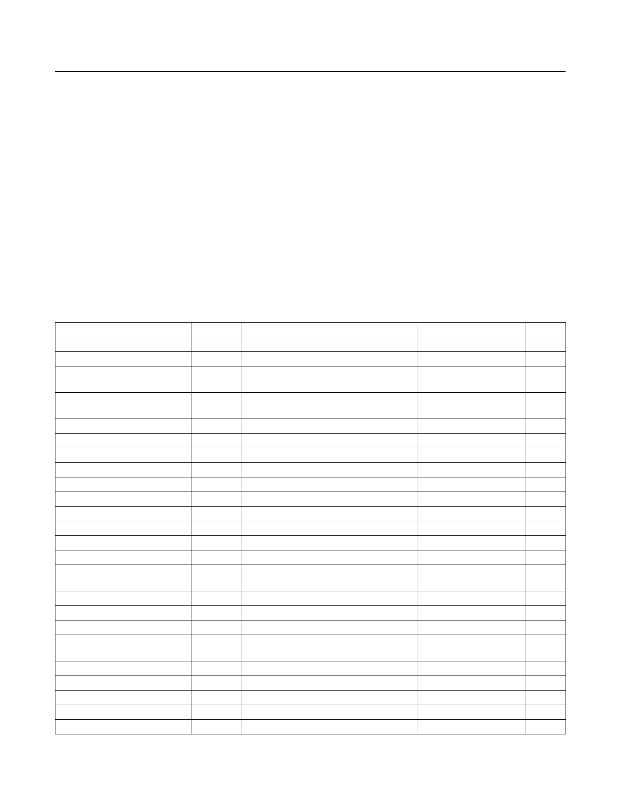
ELECTRICAL CHARACTERISTICS
(VIN = +6V, PGND = GND, CVL = 4.7µF, TA = 0°C to +85°C, unless otherwise noted. Typical values are at TA = +25°C.)
PARAMETER
SYMBOL
CONDITIONS
MIN
Input Voltage
Supply Current, No Load
VIN
3
IIN
VIN = 3V to 28V, VFB = 1.6V, SHDN = VL
Supply Current, Full Load, VL
Connected to IN
IIN
VIN = 3V to 5.5V, VFB = 1.4V, SHDN = VL = IN
TYP
500
5
MAX
28
700
6.5
Supply Current, Full Load
Shutdown Supply Current
VL Output Voltage
VL Load Regulation
VL Undervoltage Lockout
FB Set Voltage
FB Input Bias Current
Line Regulation
Load Regulation
LX Voltage
LX Switch Current Limit
Idle Mode Current-Limit
Threshold
IIN
IIN
VVL
∆VVL
VFB
IFB
∆VOUT
∆VOUT
VLX
ILXON
VIN = 3.4V to 28V, VFB = 1.4V, SHDN = VL,
VVL < VIN
VIN = 28V, VFB = 1.6V, SHDN = GND
VIN = 3.5V or 28V, no load
ILOAD = 0 to 2mA, VFB = 1.6V
Rising edge, 1% hysteresis
VFB = 1.6V
VIN = 3V to 6V, VOUT = 12V
VOUT = 12V, ILOAD = 10mA to 500mA
PWM mode
2.5
3.5
3
8
2.9
3.05
3.2
25
40
2.58
2.7
2.8
1.47
1.5
1.53
1
50
0.01 0.08
0.2
28
1.7
2.2
2.7
0.25 0.35 0.45
LX On-Resistance
LX Leakage Current
COMP Maximum Output Current
COMP Current vs. FB Voltage
Transconductance
SHDN Input Logic Low
SHDN Input Logic High
Shutdown Input Current
Switching Frequency
Maximum Duty Cycle
RLXON
ILXOFF
ICOMP
VIL
VIH
f
DC
VLX = 28V
FB = GND
∆FB = 0.1V
SHDN = GND or VL
0.3
0.6
0.02
10
100 200
0.8
1
0.8
2.0
1
200
250
300
90
95
UNITS
V
µA
mA
mA
µA
V
mV
V
V
nA
%/V
%
V
A
A
Ω
µA
µA
mmho
V
V
µA
kHz
%
2 _______________________________________________________________________________________
Share Link: 