AK4565 Просмотр технического описания (PDF) - Asahi Kasei Microdevices
Номер в каталоге
Компоненты Описание
Список матч
AK4565 Datasheet PDF : 33 Pages
| |||
ASAHI KASEI
[AK4565]
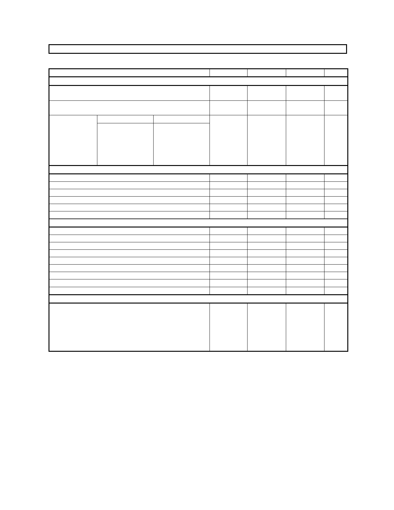
ANALOG CHARACTERISTICS
(Ta=25°C; VA, VD, VT=2.5V; fs=48kHz; Signal Frequency =1kHz; Measurement frequency = 10Hz ∼ 20kHz;
Unless otherwise specified)
Parameter
min
typ
max
Units
Input PGA Characteristics (IPGA):
Input Voltage
(INTL1-0, INTR1-0, EXTL, EXTR, LIN and RIN pins) (Note 7)
1.35
1.5
1.65
Vpp
Input Resistance: MIC (INTL1-0, INTR1-0, EXTL and EXTR pins)
6.5
LINE (LIN, RIN pins)
80
10
125
14.5
176
kΩ
Step Size
MIC
LINE
+28dB ∼ -8dB
+6dB ∼ -30dB
0.1
0.5
0.9
dB
-8dB ∼ -16dB
-30dB ∼ -38dB
0.1
1
1.9
dB
-16dB ∼ -32dB
-38dB ∼ -54dB
0.1
2
3.9
dB
-32dB ∼ -40dB
-54dB ∼ -62dB
-
2
-
dB
-40dB ∼ -52dB
-62dB ∼ -74dB
-
4
-
dB
ADC Analog Input Characteristics:
Resolution
S/(N+D)
(-2dBFS)
D-Range
(-60dBFS, A-weighted)
S/N
(A-weighted)
Interchannel Isolation (Note 9)
Interchannel Gain Mismatch
(Note 8)
20
Bits
74
83
dB
81
87
dB
81
87
dB
85
100
dB
0.2
0.5
dB
DAC Analog Output Characteristics: Measured by LOUT/ROUT
Resolution
S/(N+D)
(0dBFS)
D-Range
(-60dBFS, A-weighted)
S/N
(A-weighted)
Interchannel Isolation
Interchannel Gain Mismatch
Output Voltage (Note 10)
Load Resistance
Load Capacitance
Power Supplies
20
Bits
77
86
dB
85
91
dB
85
91
dB
85
100
dB
0.2
0.5
dB
1.35
1.5
1.65
Vpp
10
kΩ
20
pF
Power Supply Current: VA+VD+VT
Normal Operation (PDN= “H”)
All Power ON (PM3=“0”, PM2=PM1=PM0=“1”)
IPGA + ADC (PM3=PM2=“0”, PM1=PM0=“1”)
-
DAC
(PM3=“0”, PM2 = “1”, PM1=PM0=“0”)
-
Power-down mode (PDN= “L”) (Note 11)
12.5
19
mA
8.0
-
mA
5.5
-
mA
10
100
µA
Note 7. Full-scale voltage of analog inputs when IPGA is set 0dB. Its voltage is proportional to VREF. Vin = 0.6 x VREF.
Note 8. ADC measurements are input from INTL0/INTR0, INTL1/INTR1, EXTL/EXTR or LIN/RIN and routed through
IPGA. The gain of IPGA is set 0dB.
The internal HPF cancels the offset of IPGA and ADC.
Note 9. This value is interchannel isolation between INTL0 and INTR0, between INTL1 and INTR1, between EXTL
EXTR, or between LIN and RIN.
Note 10. Analog output voltage is proportional to VREF. Vout = 0.6 x VREF.
Note 11. All digital input pins except for PDN pin are held at VT or DGND. PDN pin is held at DGND.
MS0132-E-01
-6-
2003/05
Share Link: 