AD8346_ Просмотр технического описания (PDF) - Analog Devices
Номер в каталоге
Компоненты Описание
Список матч
AD8346_ Datasheet PDF : 8 Pages
| |||
AN-1039
CALIBRATION PROCEDURE
Correcting all of the modulator’s imperfections is a multistep
process. Start by looking at the procedure for LO leakage cor-
rection which results in a constellation that is offset from the
origin. A single sideband spectrum is applied to the transmitter
and is monitored on the spectrum analyzer. Next, small diffe-
rential offset voltages are applied to the I and Q inputs. Applying
differential offset voltages to the I and Q inputs should not be
confused with changing the dc bias levels (also referred to as the
common-mode level) on these pins, which has no effect. This is
done as an I offset sweep followed by a Q offset sweep (or vice
versa). Returning briefly to Figure 1, note that the AD9788 (a
16-bit, 800 MSPS dual DAC) conveniently includes two aux-
iliary DACs that can be used to couple differential dc offset
voltages on I and Q lines. This coupling is performed externally
using resistor dividers.
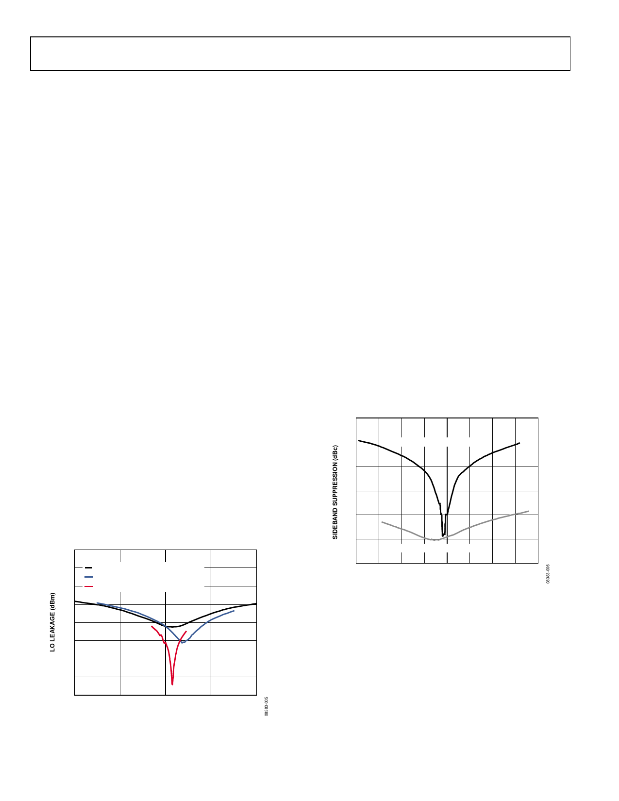
Figure 5 shows how sweeping the I and Q offset voltages alters
the LO leakage. Start by sweeping the I offset voltage around 0 V
while holding the Q offset voltage at 0 V. With modern IQ
modulators exhibiting unadjusted LO leakage in the −40 dBm
range and having voltage gains in the −5 dB to +5 dB range, an
offset voltage sweep range of ±5 mV is more than adequate to
identify the location of the null (in this example, ±2 mV is
adequate to identify a nulling voltage somewhere between
100 μV and 200 μV). Note, however, that the first pass (black
trace) only manages to reduce the LO leakage to just under
−40 dBm. This clearly indicates that the Q offset needs
correction. The second pass (blue trace) involves sweeping
the Q offset around 0 V with the I offset held at the value that
yielded the first I null. Note that a Q offset of 400 μV reduces
the LO leakage a further 10 dB to around −50 dBm. However,
a third pass is required. The trough from the first pass is quite
shallow because the Q channel had not yet been adjusted. This
makes it difficult to identify the ideal I nulling voltage. A third
pass (red trace) that involves again sweeping the I offset while
holding the Q offset at 400 μV, identifies the optimum I nulling
voltage to be 150 μV.
0
–10
FIRST PASS – I OFFSET ADJUST
SECOND PASS – Q OFFSET ADJUST
–20
THIRD PASS – I OFFSET ADJUST
–30
–40
–50
–60
–70
–80
–2
–1
0
1
2
I AND Q DIFFERENTIAL OFFSET VOLTAGES (mV)
Figure 5. Multipass LO Leakage Compensation Sweeps
Application Note
CORRECTING FOR QUADRATURE AND I/Q GAIN
ERRORS
A similar procedure can be used to correct quadrature and I/Q
gain mismatch. IQ modulator family data sheets typically specify
the quadrature phase mismatch and I/Q gain imbalance in
degrees and decibels, respectively, along with the sideband
suppression (also in decibels). Using this information, it is
advisable to perform the first optimization pass on the weaker
of the two specifications, that is, the specification which most
contributes to the sideband suppression. For example, assume
that the device data sheet specifies a sideband suppression of
−40 dBc, comprising of 1 degree of phase imbalance and 0.1 dB
of gain imbalance amplitude. In this case, it is advisable to first
try to adjust phase because making a gain adjustment has
almost no effect as long as the 1 degree of phase error is present
(see Figure 4).
Figure 6 shows the results of a gain sweep followed by a
phase sweep. In the first pass, the gain delta between I and Q
is adjusted over a range of approximately ±2 dB. The TxDAC®
in Figure 1 facilitates this adjustment by providing internal
gain adjust auxiliary DACs. The sweep yields a null of around
−57 dBc for a gain difference of approximately −0.1 dB (gain is
scaled on the top axis). Next, adjust the skew between I and Q.
This drives the null down further to −60 dBc for a phase adjust
of −0.05°.
GAIN ADJUST (dB)
–2
–1
0
1
2
–10
–20
FIRST PASS (GAIN ADJUST)
–30
–40
–50
–60
SECOND PASS (PHASE ADJUST)
–70
–0.4 –0.3 –0.2 –0.1
0
0.1 0.2 0.3 0.4
PHASE ADJUST (Degrees)
Figure 6. Multipass Sideband Suppression Compensation Sweeps
In this case, a third pass is not necessary and does not yield
further improvement. This stems from the fact that the
unadjusted phase error is very close to the optimized value
(~0.05°). Thus, the first-pass gain adjust yields a deep trough
that is only slightly improved during the phase sweep. This
contrasts to the LO leakage nulling where a third pass yielded
further improvement.
Rev. 0 | Page 6 of 8
Share Link: 