ADL5571-EVALZ Просмотр технического описания (PDF) - Analog Devices
Номер в каталоге
Компоненты Описание
Список матч
ADL5571-EVALZ Datasheet PDF : 16 Pages
| |||
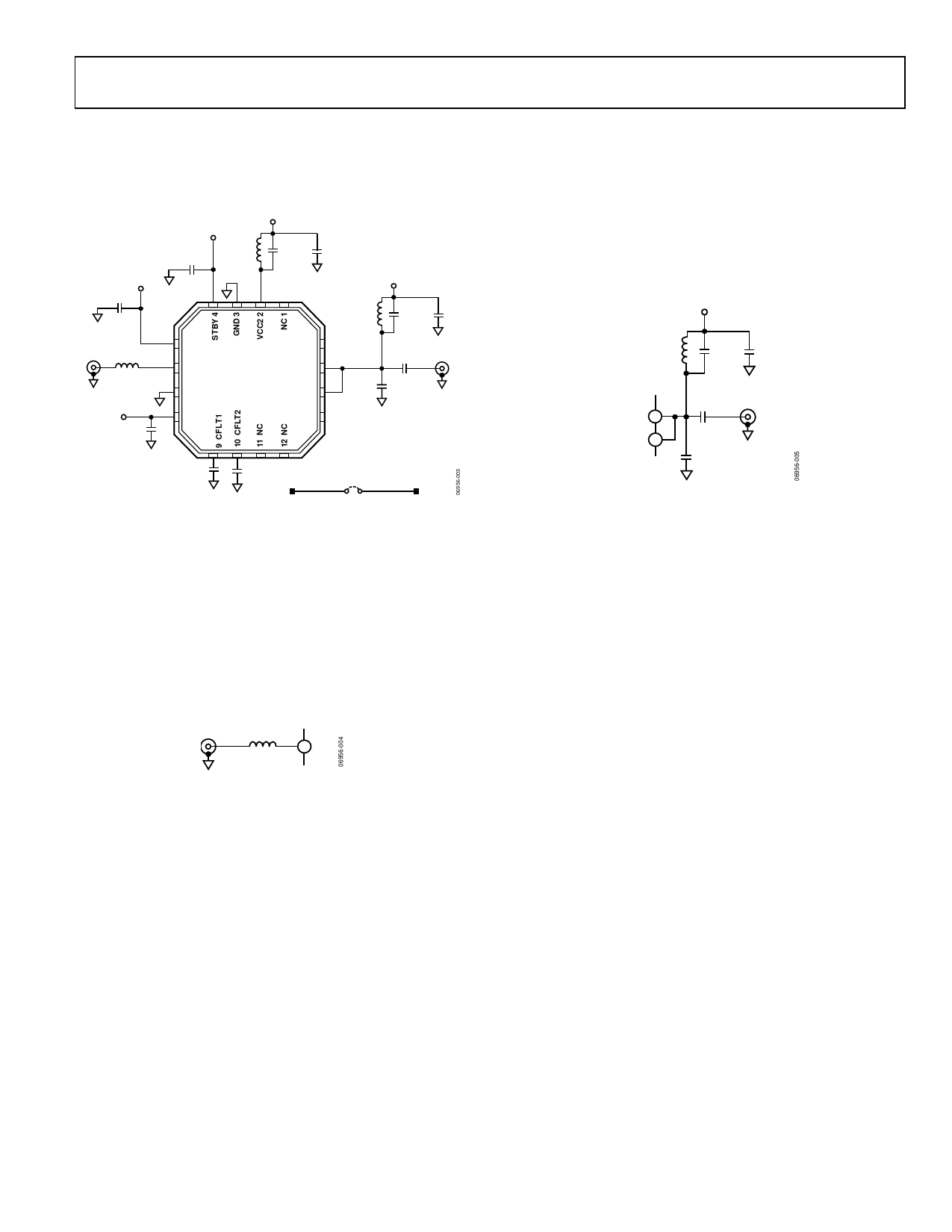
APPLICATIONS INFORMATION
BASIC CONNECTIONS
Figure 19 shows the basic connections for the ADL5571.
VPOS
C7
0.01µF
VPOS
STBY
L1
C6
C11
C8
1nH
3.3pF
1µF
0.01µF
VPOS1
L2
11nH
C5
C12
OPEN
1µF
RFIN L3
2.7nH
VREG
C9
0.01µF
5 VCC1
NC 16
6 RFIN
7 GND
RFOUT 15
ADL5571
RFOUT 14
8 VREG
NC 13
C3
2.7pF
C4 RFOUT
39pF
C2
C10
2.2pF
0.01µF
VPOS1
W1
VPOS
NC = NO CONNECT
Figure 19. Basic Connections
Power Supply
The voltage supply on the ADL5571, which ranges from
3.2 V to 4.2 V, should be connected to the VCCx pins. VCC1 is
decoupled with Capacitor C7, whereas VCC2 uses a tank circuit
to prevent RF signals from propagating on the dc lines.
RF Input Interface
The RFIN pin is the port for the RF input signal to the power
amplifier. The L3 inductor, 2.7 nH, matches the input
impedance to 50 Ω.
2.7nH
L3
6 RFIN
Figure 20. RF Input with Matching Component
ADL5571
RF Output Interface
The parallel RF output ports have a shunt capacitor, C3 (2.7 pF),
and the line inductance of the microstrip line for optimized
output power and linearity. The characteristics of the ADL5571
are described for 50 Ω impedance after the output matching
capacitor (load after C3). C4 provides dc blocking on the
RF output.
VPOS1
L2
11nH
C5
C12
OPEN 1µF
RFOUT 15
RFOUT 14
C4
39pF
C3
2.7pF
RFOUT
Figure 21. RF Output
Transmit/Standby Enable
During normal transmit mode, the STBY pin is biased low
(0 V). However, during receive mode, the pin can be biased
high (2.5 V) to shift the device into standby mode, which
reduces current consumption to 9 mA.
VREG Enable
During normal transmit, the VREG pin is biased to 2.85 V and
draws 9 mA of current. When the VREG pin is low (0 V), the
device suspends itself into sleep mode (irrespective of supply
biasing). In this mode, the device draws less than 1 μA of
current.
Rev. 0 | Page 11 of 16
Share Link: 