ADL5570 Просмотр технического описания (PDF) - Analog Devices
Номер в каталоге
Компоненты Описание
Список матч
ADL5570 Datasheet PDF : 12 Pages
| |||
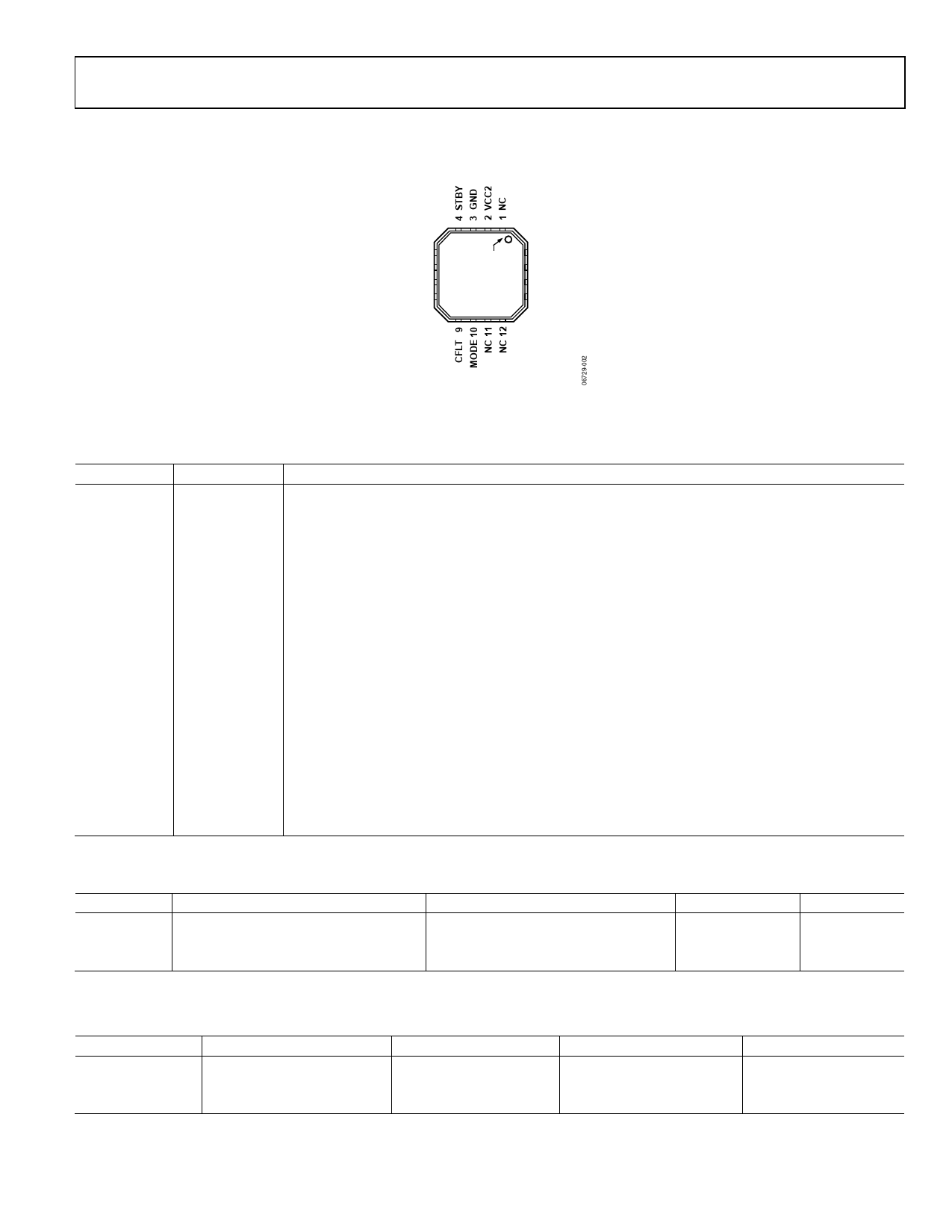
PIN CONFIGURATION AND FUNCTION DESCRIPTIONS
ADL5570
VCC1 5
RFIN 6
GND 7
VREG 8
PIN 1
INDICATOR
ADL5570
TOP VIEW
(Not to Scale)
16 NC
15 RFOUT
14 RFOUT
13 NC
NC = NO CONNECT
Figure 2. Pin Configuration
Table 3. Pin Function Descriptions
Pin No.
Mnemonic
Description
1, 11 to 13, 16 NC
No Connect. Do not connect these pins.
2
VCC2
This power supply pin should be connected to the supply via a choke circuit (see Figure 10).
3, 7
GND
Connected to Ground.
4
STBY
When STBY is low (0 V), the device operates in transmit mode. When the radio is receiving data,
STBY can be taken high (2.5 V), reducing supply current to 1 mA.
5
VCC1
Connect to Power Supply.
6
RFIN
Matched RF Input.
8
VREG
When VREG is low, the device goes into sleep mode, reducing supply current to 10 μA. When VREG
is high (2.85 V), the device operates in its normal transmit mode. When high, VREG draws a bias
current of approximately 10 mA.
9
CFLT
A ground-referenced capacitor should be connected to this pin to reduce bias line noise (see Figure 10).
10
MODE
Switches Between High Power and Low Power Modes. When MODE is low (0 V), the device operates
in high power mode. When MODE is high (2.5 V), the device operates in low power mode. See Table 4
for appropriate biasing. In cases where the MODE feature is not used, this pin should be connected
to ground through a 50 kΩ resistor.
14, 15
RFOUT
Unmatched RF Output. These parallel outputs can be matched to 50 Ω using strip-line and shunt
capacitance. The power supply voltage should be connected to these pins through a choke inductor.
Exposed Paddle The exposed paddle should be soldered down to a low impedance ground plane (if multiple
ground layers are present, use multiple vias (9 minimum) to stitch together the ground planes) for
optimum electrical and thermal performance.
Table 4. VCC = 3.5 V Operating Modes1
Mnemonic High Power Mode, POUT > 10 dBm
VREG
High
MODE
Low
STBY
Low
1 X = don’t care.
Low Power Mode, POUT ≤ 10 dBm
High
High
Low
Standby Mode
High
X
High
Sleep Mode
Low
X
X
Table 5. VREG, MODE, and STBY Pins
Mnemonic
Nominal High (V)
VREG
2.85
MODE
2.5
STBY
2.5
High Range (V)
2.75 to 2.95
>2.4
>2.4
Nominal Low (V)
0
0
0
Low Range (V)
NA
<1
<1
Rev. 0 | Page 5 of 12
Share Link: 