ADL5570-EVALZ Просмотр технического описания (PDF) - Analog Devices
Номер в каталоге
Компоненты Описание
Список матч
ADL5570-EVALZ Datasheet PDF : 12 Pages
| |||
FEATURES
Fixed gain of 29 dB
Operation from 2.3 GHz to 2.4 GHz
EVM ≤ 3% at POUT = 25 dBm with 16 QAM OFDMA
Input internally matched to 50 Ω
Power supply: 3.2 V to 4.2 V
Quiescent current
130 mA in high power mode
70 mA in low power mode
Power-added efficiency (PAE): 20%
Multiple operating modes to reduce battery drain
Low power mode: 100 mA
Standby mode: 1mA
Sleep mode: <1 μA
APPLICATIONS
WiMAX/WiBro mobile terminals
GENERAL DESCRIPTION
The ADL5570 is a high linearity 2.3 GHz to 2.4 GHz power
amplifier designed for WiMAX terminals using TDD operation
at a duty cycle of 31%. With a gain of 29 dB and an output
compression point of 31 dBm at 2.35 GHz, it can operate at
an output power level up to 26 dBm while maintaining an EVM
of ≤3% (OFDM 16 or 64 QAM) with a supply voltage of 3.5 V.
PAE is 20% @ POUT = 25 dBm.
The ADL5570 RF input is matched on-chip and provides an
input return loss of less than −10 dB. The open-collector output is
externally matched with strip-line and external shunt capacitance.
2.3 GHz to 2.4 GHz
WiMAX Power Amplifier
ADL5570
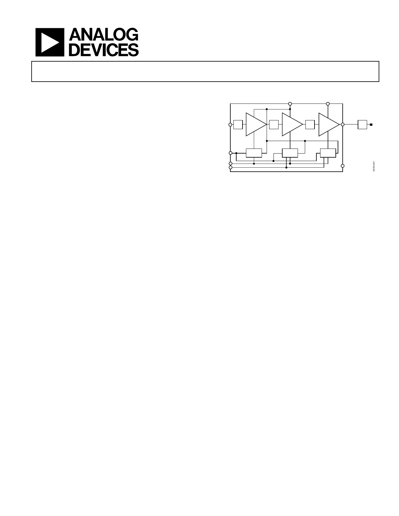
FUNCTIONAL BLOCK DIAGRAM
VCC1
VCC2
RFIN
IM1
FIRST
STAGE
IM2
SECOND
STAGE
IM3
THIRD
STAGE
RFOUT
OM
STBY
VREG
MODE
BIAS_1
BIAS_2
Figure 1.
BIAS_3
CFLT
The ADL5570 operates over a supply voltage range from 3.2 V
to 4.2 V with a supply current of 440 mA burst rms when
delivering 25 dBm (3.5 V supply). A low power mode is also
available for operation at power levels of ≤10 dBm with
optimized operating and quiescent currents of 100 mA and
70 mA, respectively. A standby mode is available that reduces
the quiescent current to 1 mA, which is useful when a TDD
terminal is receiving data.
The ADL5570 is fabricated in a GaAs HBT process and is packaged
in a 4 mm × 4 mm, 16-lead, Pb-free RoHS-compliant LFCSP
that uses an exposed paddle for excellent thermal impedance.
It operates from −40°C to +85°C.
Rev. 0
Information furnished by Analog Devices is believed to be accurate and reliable. However, no
responsibility is assumed by Analog Devices for its use, nor for any infringements of patents or other
rights of third parties that may result from its use. Specifications subject to change without notice. No
license is granted by implication or otherwise under any patent or patent rights of Analog Devices.
Trademarks and registered trademarks are the property of their respective owners.
One Technology Way, P.O. Box 9106, Norwood, MA 02062-9106, U.S.A.
Tel: 781.329.4700
www.analog.com
Fax: 781.461.3113
©2007 Analog Devices, Inc. All rights reserved.
Share Link: 