ADL5370(RevA) Просмотр технического описания (PDF) - Analog Devices
Номер в каталоге
Компоненты Описание
Список матч
ADL5370 Datasheet PDF : 20 Pages
| |||
Data Sheet
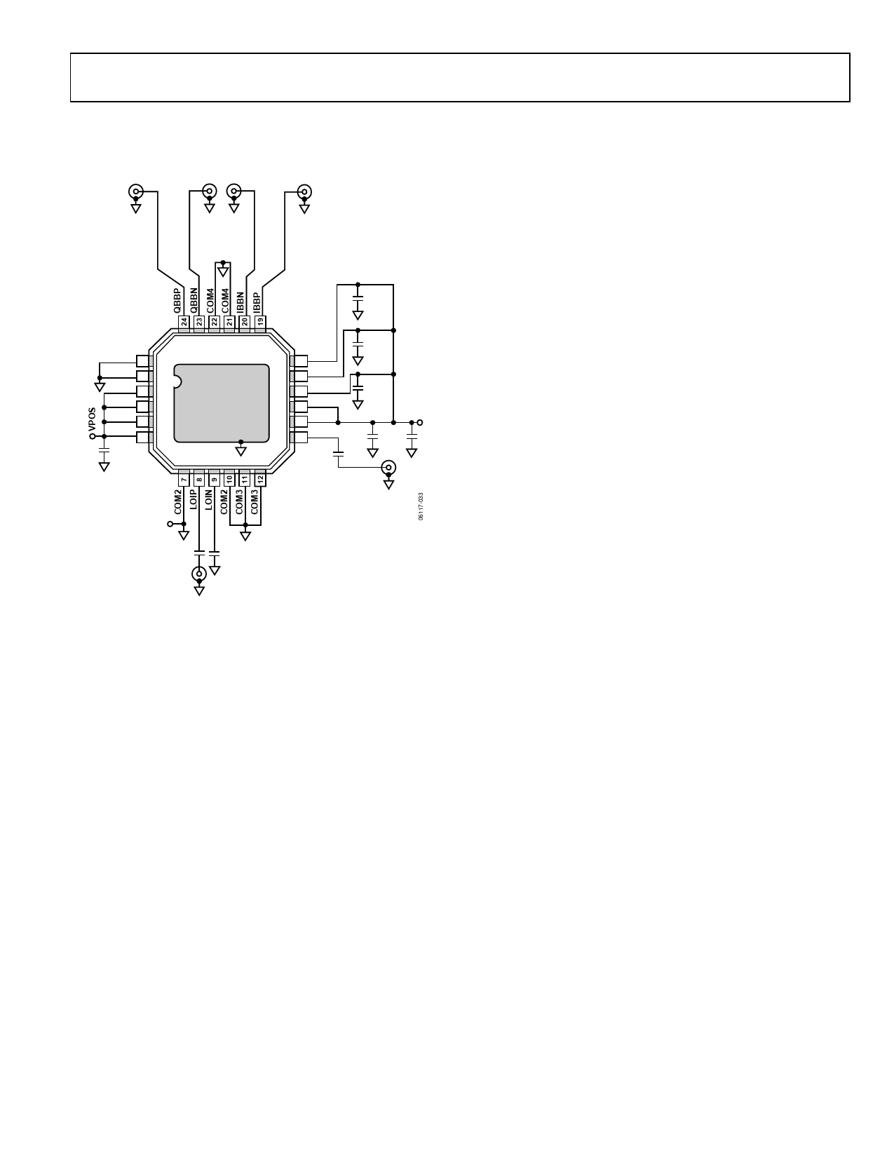
BASIC CONNECTIONS
Figure 25 shows the basic connections for the ADL5370.
QBBP
QBBN IBBN
IBBP
C16
0.1µF
COM1 1
COM1 2
VPS1 3
VPS1 4
VPS1 5
VPS1 6
C12
0.1µF
Z1
ADL5370
EXPOSED
PADDLE
18 VPS5
C15
0.1µF
17 VPS4
16 VPS3
C14
0.1µF
15 VPS2
14 VPS2
VPOS
13
VOUT
C13
0.1µF
C11
OPEN
COUT
100pF
VOUT
GND
CLOP
100pF
LO
CLON
100pF
Figure 25. Basic Connections for the ADL5370
Power Supply and Grounding
All the VPS pins must be connected to the same 5 V source.
Adjacent pins of the same name can be tied together and
decoupled with a 0.1 µF capacitor. These capacitors should be
located as close as possible to the device. The power supply can
range between 4.75 V and 5.25 V.
The COM1 pin, COM2 pin, COM3 pin, and COM4 pin should
be tied to the same ground plane through low impedance paths.
The exposed paddle on the underside of the package should also
be soldered to a low thermal and electrical impedance ground
plane. If the ground plane spans multiple layers on the circuit
board, they should be stitched together with nine vias under the
exposed paddle. The Analog Devices application note, AN-772,
discusses the thermal and electrical grounding of the LFCSP in
detail.
ADL5370
Baseband Inputs
The baseband inputs QBBP, QBBN, IBBP, and IBBN must be
driven from a differential source. The nominal drive level of
1.4 V p-p differential (700 mV p-p on each pin) should be
biased to a common-mode level of 500 mV dc.
The dc common-mode bias level for the baseband inputs may
range from 400 mV to 600 mV. This results in a reduction in the
usable input ac swing range. The nominal dc bias of 500 mV allows
for the largest ac swing, limited on the bottom end by the ADL5370
input range and on the top end by the output compliance range on
most digital-to-analog converters (DAC) from Analog Devices.
LO Input
A single-ended LO signal should be applied to the LOIP pin
through an ac-coupling capacitor. The recommended LO drive
power is 0 dBm. The LO return pin, LOIN, should be ac-coupled
to ground through a low impedance path.
The nominal LO drive of 0 dBm can be increased to up to 7 dBm
to realize an improvement in the noise performance of the
modulator. This improvement is tempered by degradation in
the sideband suppression performance (see Figure 20) and,
therefore, should be used judiciously. If the LO source cannot
provide the 0 dBm level, then operation at a reduced power
below 0 dBm is acceptable. Reduced LO drive results in slightly
increased modulator noise. The effect of LO power on sideband
suppression and carrier feedthrough is shown in Figure 20. The
effect of LO power on GSM noise is shown in Figure 35.
RF Output
The RF output is available at the VOUT pin (Pin 13). This pin
must also be ac-coupled. The VOUT pin has a nominal broadband
impedance of 50 Ω and does not need further external matching.
Rev. A | Page 11 of 20
Share Link: 