ADL5322ACPZ-WP(Rev0) Просмотр технического описания (PDF) - Analog Devices
Номер в каталоге
Компоненты Описание
Список матч
ADL5322ACPZ-WP Datasheet PDF : 12 Pages
| |||
ADL5322
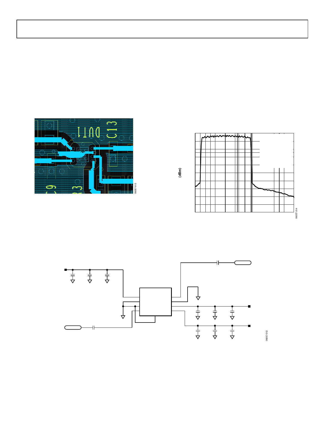
BASIC CONNECTIONS
Figure 14 shows the basic connections for operating the
ADL5322. Each of the three power supply lines should be
decoupled with 10 μF, 10 nF, and 100 pF capacitors. Pin 3, Pin 6,
Pin 7, and the exposed paddle under the device should all be
connected to a low impedance ground plane. If multiple ground
planes are being used, these should be stitched together with
vias under the device to optimize thermal conduction. See
recommended land pattern in Figure 12.
Figure 12. Recommended Land Pattern
CDMA2000 DRIVING APPLICATION
Figure 13 shows a plot of the spectrum of an ADL5323 driving
at 4-carrier CDMA2000 signal at 0 dBm per carrier (total
carrier power = 6 dBm), centered at 880 MHz. At 750 kHz
and 1.98 MHz offset, adjacent channel power ratios of −59 dBc
and −84 dBc (measured in 30 kHz with respect to the 1.22 MHz
carrier) are observed. At 4 MHz carrier offset, −73 dBc is
measured in a 1 MHz bandwidth (−133 dBm/Hz). Note that
the spectrum of the four carriers is slightly rounded due the
frequency response of the cavity-tuned filter that was used to
filter out the noise and distortion of the source signal.
–10
RBW = 30kHz
–20
VBW = 300kHz
SWT = 2s
RF ATT = 20dB
–30
MIXER = –10dBm
–40
CH PWR = 0.26dBm
ACP UP = –59.33dB
ALT1 UP = –84.35dB
–50
ALT2 UP = –72.74dB
–60
–70
–80
–90
–100
–110
CENTER 881.875MHz
1MHz/
SPAN 10MHz
Figure 13. Spectrum of 4 Adjacent CDMA2000 Carriers Centered at 880 MHz;
Total Carrier Power = 6 dBm (0 dBm per Carrier)
VCC
C1
10µF
AGND
C3
10nF
AGND
C2
100pF
AGND
RFIN
C4
100pF
AGND
C5
100pF
RFOUT
ADL5322
5 VCC
6 GND
RFOUT 4
GND 3
7 GND
VCC 2
8 RFIN
VCC 1
EP
Figure 14. Basic Connections
AGND
C6
100pF
AGND
C7
10nF
AGND
C9
100pF
AGND
C10
10nF
AGND
C8
10µF
AGND
C11
10µF
AGND
VCC
VCC
Rev. 0 | Page 8 of 12
Share Link: 