ADJD-S313-QR999 Просмотр технического описания (PDF) - Avago Technologies
Номер в каталоге
Компоненты Описание
Список матч
ADJD-S313-QR999 Datasheet PDF : 16 Pages
| |||
In the case of the master-receiver and slave-
transmitter, the master generates a not
acknowledge to signal the end of the data transfer
to the slave-transmitter. The master can then send
a STOP or repeated START condition to begin a new
data transfer.
In all cases, the master generates the acknowledge
or not acknowledge SCL clock pulse.
Addressing
Each slave device on the serial bus needs to have a
unique address. This is the first byte that is sent by
the master-transmitter after the START condition.
The address is defined as the first seven bits of the
first byte.
The eighth bit or least significant bit (LSB)
determines the direction of data transfer. A ‘one’
in the LSB of the first byte indicates that the master
will read data from the addressed slave (master-
receiver and slave-transmitter). A ‘zero’ in this
position indicates that the master will write data
to the addressed slave (master-transmitter and
slave-receiver).
A device whose address matches the address sent
by the master will respond with an acknowledge
for the first byte and set itself up as a slave-
transmitter or slave-receiver depending on the LSB
of the first byte.
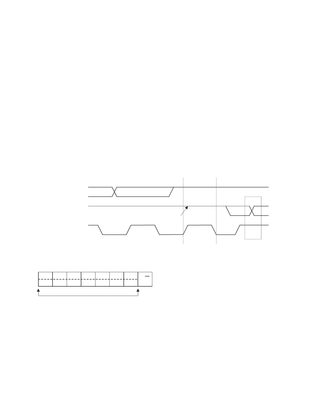
The slave address on ADJD-S313 is 0x58 (7-bits).
SDA
(SLAVE-TRANSMITTER)
SDA
(MASTER-RECEIVER)
SCL
(MASTER)
Figure 6. Master-Receiver Acknowledge
LSB
SDA left HIGH
by transmitter
SDA left HIGH
by receiver
8
Not
acknowledge
9
Acknowledge
clock pulse
MSB
LSB
A6 A5 A4 A3 A2 A1 A0
R/W
1
0
1
1
0
0
0
Slave address
Figure 7. Slave Addressing
P
Sr
STOP or repeated
START condition
10
Share Link: 