AD9713BAN Просмотр технического описания (PDF) - Fairchild Semiconductor
Номер в каталоге
Компоненты Описание
Список матч
AD9713BAN Datasheet PDF : 17 Pages
| |||
mends that these references (VFT & VFB) be operated to
within ± 2% (or ± 2.5 V ± 50 mV) to maintain accuracy within
the specified limit. Before each EB7820/24 board is shipped,
the references are adjusted for VFT and VFB of ±2.5 V ±5 mV
respectively. For each new SPT7820 or SPT7824, VST and
VSB need to be readjusted. All measurement must be
referenced to AGND test point (provided).
REFERENCE MONITORING
Table 2 - Recommended Operating Voltage Range
Monitoring
Ref
Point
VST U1, PIN 20
VSB U1, PIN 23
Min
+1.95 V
- 2.05 V
Typ Max Adjust
+2.00 V +2.05 V R1
- 2.00 V - 1.95 V R2
Note that the SPT7820 and SPT7824 (especially refer-
ence taps VFT VFB, VST and VRM) are sensitive to
electrostatic discharge (ESD).
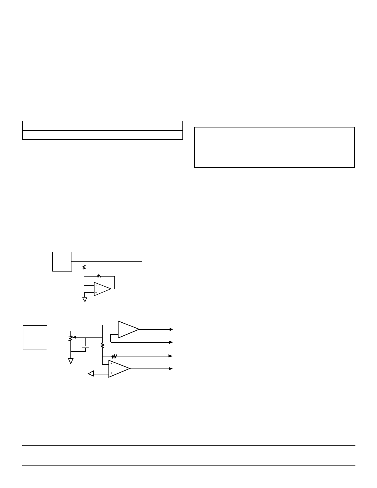
Figure 4A shows one type of reference driver. Figure 4B is
another way to drive the reference circuits using force and
sense. The alternate circuit provides better control of plus
full scale (+FS) and minus full scale (-FS) errors by sensing
VST and VSB to ± 2.0 V respectively. However, the refer-
ence pins VST and VSB are not low impedance nodes that
require additional precaution when routing (PCB layout).
Figure 4A - Reference Driver
REF-03
R
R
-
+OP-07
VFT
-2.5 V
VFB
Figure 4B - Alternative Reference Driver
OUT
REF-03
+2.5 V
10 k
+2.0 V
0.1
10 k
+
OP-07
-
10 k
-
+OP-07
≈ +2.5 V VFT
+2.0 V VST
-2.0 V VSB
≈ -2.5 V VFB
SPT7820 OR SPT7824, 10-BIT ADC
The SPT7820 integrated circuit is a 10-bit analog-to-digital
converter capable of digitizing an input signal with a minimum
update rate of 20 mega-samples per second (MSPS). The
SPT7824, on the other hand is pin compatible with the
SPT7820 except that it is faster: 40 MSPS for the sampling
frequency. On both devices, the expected full scale analog
input range is from VST to VSB. The analog input is latched
at the leading edge of the CLK. There are 11 digital TTL
outputs. D0 - D9 are the parallel TTL-output bits, with D0 the
LSB, D9 the MSB and D10 the overrange bit. The data
outputs are latched at the rising edge of the CLK, with a
propagation delay of typically 14 nsec. There is one clock
latency between CLK and valid output data (see figure 5 for
more detail). The output code is a straight binary:
Table 3: SPT7820/24 Output Coding
(Ø Indicates the Flickering Bit Between Logic 0 and 1)
Analog Input
D12 (Overrange Bit) Data Output Code
<- 2.0 V
0
OO OOOO OOOO
- 2.0 V +1 LSB
0
OO OOOO OOOØ
0V
0
ØØ ØØØØ ØØØØ
+ 2.0 V - 1 LSB
0
11 1111 111Ø
> + 2.0 V + 1/2 LSB
1
11 1111 1111
Pin 21 is the analog input pin. Selecting the analog input
driver for the SPT7820/24 is less of an issue than with most
Flash ADCs because the input impedance and input capaci-
tance are typically 300 kΩ and 5 pF, respectively. For
example, at 10 MHz and 4 VP-P sinewave input, the input
driver source only requires 0.648 mA of peak output current
(4 πFC).
The analog input is directly fed from a BNC (VIN). R10 (51
Ω), analog input source termination is mounted on a socket
as a user-selectable termination. The analog input pin has
no circuit protection. Its maximum rating is from VFT to VFB
(±2.5 V). In an application in which the analog input range is
greater than ±2.5 V, protect the input pin from permanent
damage with a voltage limiter.
INPUT CLOCK DRIVER
CLK is the single-ended input clock to the EB7820/24 (evalu-
ation board), CLK IN is the input clock to the SPT7820 or
SPT7824, and CCLK is the capture clock used for the output
latches (U7 & U8).
The clock input of the SPT7820/24 requires a TTL-logic level
of 6 nsec or faster to improve the noise. TTL-logic family
(74FXX) is good for driving the SPT7820/24. Finding a TTL-
square wave generator up to 40 MHz with fast slew rate and
low jitter is harder than a sine wave, low jitter generator. U5
(MAX9686, TTL-voltage comparator) provides most of the
above requirements to drive the SPT7820 or SPT7824 (ex-
cept the low jitter generator). The CLK signal can be a sine
wave signal with the amplitude not to exceed ± 3 V (input
common mode limitation of U5). R11 (51 Ω) is the CLK
source termination. Use R3 to adjust the duty cycle of the
CLK IN. CLK IN is in phase with CLK and has a a propagation
delay of 6 nsec typically. The positive clock (CLK IN) pulse
width must be kept between 10 nsec and 300 nsec for the
AN7820/24
3
5/22/97
Share Link: 