AD8349ARE(REV0) Просмотр технического описания (PDF) - Analog Devices
Номер в каталоге
Компоненты Описание
Список матч
AD8349ARE Datasheet PDF : 28 Pages
| |||
AD8349
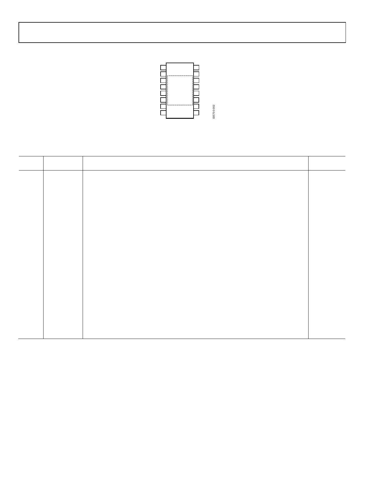
PIN CONFIGURATION AND FUNCTIONAL DESCRIPTIONS
IBBP 1 AD8349 16 QBBP
IBBN 2
15 QBBN
COM1 3 TOP VIEW 14 COM3
COM1 4 (Not to Scale) 13 COM3
LOIN 5
12 VPS2
LOIP 6
11 VOUT
VPS1 7
10 COM3
ENOP 8
9 COM2
Figure 2
Table 3. Pin Function Descriptions
Pin No. Mnemonic
1, 2,
IBBP, IBBN,
15, 16 QBBN, QBBP
3, 4
COM1
5, 6
LOIN, LOIP
7
VPS1
8
ENOP
9
COM2
10, 13,
14
11
COM3
VOUT
12
VPS2
Description
Differential In-Phase and Quadrature Baseband Inputs. These high impedance inputs must be
dc-biased to approximately 400 mV dc, and must be driven from a low impedance source.
Nominal characterized ac signal swing is 600 mV p-p on each pin (100 mV to 700 mV). This
results in a differential drive of 1.2 V p-p with a 400 mV dc bias. These inputs are not self-biased
and must be externally biased.
Common Pin for LO Phase Splitter and LO Buffers. COM1, COM2, and COM3 should all be
connected to a ground plane via a low impedance path.
Differential Local Oscillator Inputs. Internally dc-biased to approximately 1.8 V when VS = 5.0 V.
Pins must be ac-coupled. Single-ended drive is possible with degradation in performance.
Positive Supply Voltage (4.75 V to 5.25 V) for the LO Bias-Cell and Buffer. VPS1 and VPS2 should
be connected to the same supply. To ensure adequate external bypassing, connect 0.1 µF and
100 pF capacitors between VPS1 and ground.
Output Enable. This pin can be used to enable or disable the RF output. Connect to high logic
level for normal operation. Connect to low logic level to disable output.
Common Pin for the Output Amplifier. COM1, COM2, and COM3 should all be connected to a
ground plane via a low impedance path.
Common Pin for Input V-to-I Converters and Mixer Cores. COM1, COM2, and COM3 should all
be connected to a ground plane via a low impedance path.
Device Output. Single-ended, 50 Ω internally biased RF output. Pin must be ac-coupled to the
load.
Positive Supply Voltage (4.75 V to 5.25 V) for the Baseband Input V-to-I Converters, Mixer Core,
Band Gap Reference, and Output Amplifer. VPS1 and VPS2 should be connected to the same
supply. To ensure adequate external bypassing, connect 0.1 µF and 100 pF capacitors between
VPS2 and ground.
Equivalent
Circuit
Circuit A
Circuit B
Circuit C
Circuit D
Rev. 0 | Page 6 of 28
Share Link: 