AD8340ACPZ-REEL7 Просмотр технического описания (PDF) - Analog Devices
Номер в каталоге
Компоненты Описание
Список матч
AD8340ACPZ-REEL7 Datasheet PDF : 20 Pages
| |||
Data Sheet
AD8340
BS, 1X, C0 : ADJ CHANNE L
REF –12dBm
OFFSET 0.5 dB
–20
*ATT 5dB
–30
–40
–50
*RBW 30kHz
*VBW 30kHz
*SWT 100ms
MARKER 2 [T1 NOI]
–148.76dBm/Hz
876.009615385MHz
CH PWR –5.17dBm
ACP LOW –60.94dB
ACP UP –60.08dB
ALT1 LOW –86.40dB
ALT1 UP –86.80dB
MARKER 1 [T1 NOI]
–148.89dBm/Hz
884.006410256MHz
LVL
NOR
–60
SWP 50 OF 50
–70
–80
–90
10
–50
0
POUT vs. VIN
–55
–10
–60
–20
ACP – 750kHz OFFSET, 30kHz RBW
–65
–30
–70
–40
–75
ACP – 1.98MHz OFFSET, 30kHz RBW
–50
–80
–60
NOISE – 4MHz OFFSET, 1MHz RBW
–85
–100
2
1
–110
CENTER 880MHz
1MHz/DIV
SPAN 10MHz
Figure 35. Output Spectrum, Single-Carrier CDMA2000 Test Model at −5 dBm
VI = VQ = 0.353 V, ACP Measured at 750 kHz and 1.98 MHz Carrier Offset,
Noise Measured at ±4 MHz Carrier Offset, Input Signal Filtered Using a
Cavity Tuned Filter (Pass Band = 4.6 MHz)
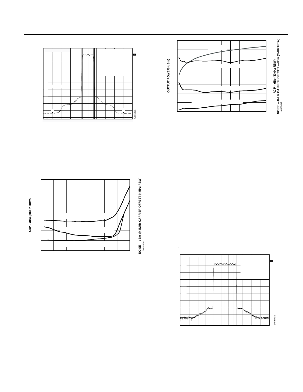
Holding the I and Q control voltages steady at 0.353 V, input
power was swept. Figure 36 shows the resulting output power,
noise floor, and adjacent channel power ratio. Noise floor is
presented as noise in a 1 MHz bandwidth as defined by the
3GPP2 specification.
–30
–30
–40
–40
–50
–50
–60
–60
ACP – 750kHz OFFSET, 30kHz RBW
–70
–70
–80
ACP – 1.98MHz OFFSET, 30kHz RBW
–80
–90
–90
NOISE – 4MHz OFFSET, 1MHz RBW
–100
–30
–25
–20
–15
–10
–5
0
OUTPUT POWER (dBm)
–100
5
Figure 36. Noise and ACP vs. Output Power,
Single-Carrier CDMA2000 Test Model, VI = VQ = 0.353,
ACP Measured in 30 kHz RBW at ±750 kHz and ±1.98 MHz Carrier Offset,
Noise Measured at ±4 MHz Carrier Offset
–70
0
–90
50 100 150 200 250 300 350 400 450 500
VI = VQ =VIN (mV)
Figure 37. Output Power, Noise, and ACP vs. I and Q Control Voltages,
CDMA2000 Test Model, VI = VQ, ACP Measured in 30 kHz RBW at ±750 kHz
and ±1.98 MHz Carrier Offset, Noise Measured at ±4 MHz Carrier Offset
In contrast to Figure 36, Figure 37 shows that for a fixed input
power, ACP remains fairly constant as gain and phase are
changed (this is not true for very high input powers). The noise
floor still drops with decreasing gain, but it never reaches the
−90 dBm level shown in Figure 37.
Figure 38 shows the output spectrum for a 3-carrier CDMA2000
spectrum. Again, the signal being applied to the AD8340 is
filtered by a cavity-tuned filter with a −3 dB bandwidth of
4.6 MHz. To reduce distortion, the total output carrier power
was reduced to approximately −8 dBm (per-carrier power =
−12.6 dBm). Adjacent channel power ratios of −61 dBc (2 MHz
from center of spectrum) and −82 dBc (3.23 MHz from center
of spectrum) were measured. The noise floor, measured at
5.25 MHz carrier offset, is approximately −149 dBm/Hz (−89 dBm
in a 1 MHz bandwidth). While some dynamic range is lost due
to output power back-off, ACP stays approximately equal and
noise floor improves slightly.
REF –15 dBm
*ATT 5dB
OFFSET 0.5dB
–20
–30
–40
–50
*RBW 30kHz
*VBW 300kHz
*SWT 5s
MARKER 1 [T1 NOI]
–148.83dBm/Hz
885.252403846MHz
CH1
–12.65dBm
CH2
CH3
TOTAL
–12.58dB
–12.87dB
–7.93dB
A
SOL
ACP LOW –61.41dB
ACP UP –61.87dB LVL
ALT1 LOW –82.36dB
ALT1 UP –81.92dB NOR
The results show that at an output power of 3 dBm, ACP is still
in compliance with the standard (<−45 dBc at 750 MHz and
<−60 dBc at 1.98 MHz). At low output power levels, ACP at
1.98 MHz, carrier offset degrades as the noise floor of the
AD8340 becomes the dominant contributor to measured ACP.
Measured noise at 4 MHz carrier offset begins to increase
sharply above 0 dBm output power. This increase is not due to noise.
but results from increased carrier-induced distortion. As output
power drops below 0 dBm, the noise floor drops towards −90 dBm.
With a fixed input power of 2.4 dBm, the output power was
again swept by exercising the I and Q inputs. VI and VQ were
kept equal and were swept from 10 mV to 500 mV. The
resulting output power, ACP, and noise floor are shown in
Figure 37.
–60
–70
–80
–90
–100
1
–110
CENTER 880MHz
1.5MHz/
SPAN 15MHz
Figure 38. Output Spectrum, 3-Carrier CDMA2000 Test Model at
−12.5 dBm/Carrier, VI = VQ = 0.353 V, ACP Measured at 2 MHz and 3.23 kHz
Offset from Center of Spectrum, Noise Measured at 5.25 MHz Carrier Offset,
Input Signal Filtered Using a Cavity-Tuned Filter (Pass Band = 4.6 MHz)
Rev. C | Page 15 of 20
Share Link: 