AD8340(2004) Просмотр технического описания (PDF) - Analog Devices
Номер в каталоге
Компоненты Описание
Список матч
AD8340 Datasheet PDF : 20 Pages
| |||
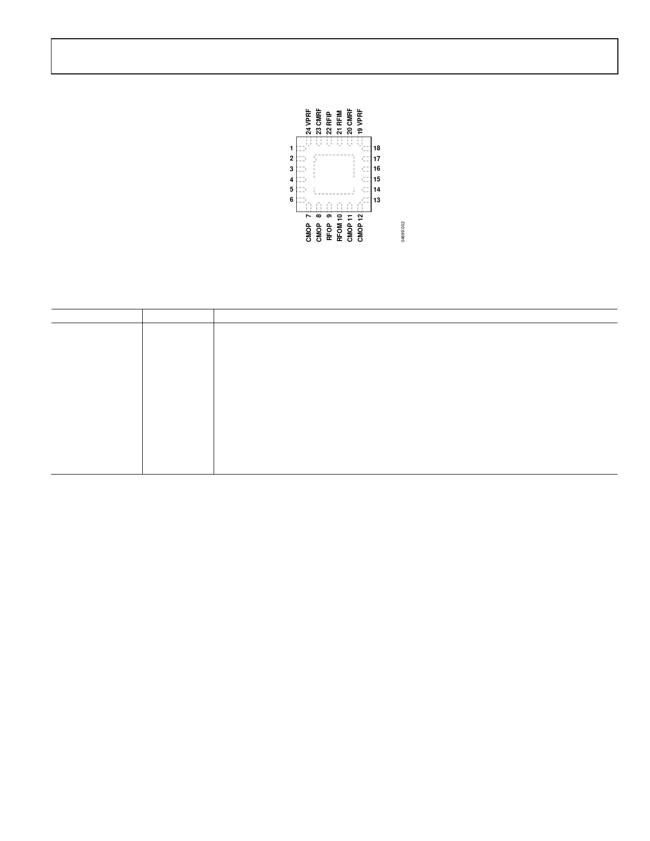
PIN CONFIGURATION AND FUNCTION DESCRIPTIONS
AD8340
QFLP 1
QFLM 2
QBBP 3
QBBM 4
VPS2 5
VPS2 6
PIN 1
INDICATOR
AD8340
TOP VIEW
(Not to Scale)
18 IFLP
17 IFLM
16 IBBP
15 IBBM
14 VPS2
13 DSOP
Table 3. Pin Function Descriptions
Pin No.
Mnemonic
1, 2
QFLP, QFLM
3, 4
5, 6, 14, 19, 24
7, 8, 11, 12, 20, 23
9, 10
13
15, 16
17, 18
QBBP, QBBM
VPS2, VPRF
CMOP, CMRF
RFOP, RFOM
DSOP
IBBM, IBBP
IFLM, IFLP
21, 22
RFIM, RFIP
Figure 2. 24-Lead Lead Frame Chip Scale Package (LFCSP)
Function
Q Baseband Input Filter Pins. Connect optional capacitor to reduce Q baseband channel low-pass
corner frequency.
Q Channel Differential Baseband Inputs.
Positive Supply Voltage. 4.75 V − 5.25 V.
Device Common. Connect via lowest possible impedance to external circuit common.
Differential RF Outputs. Must be ac-coupled. Differential impedance 50 Ω nominal.
Output disable. Pull high to disable output stage.
I Channel Differential Baseband Inputs.
I Baseband Input Filter Pins. Connect optional capacitor to reduce I baseband channel low-pass
corner frequency.
Differential RF Inputs. Must be ac-coupled. Differential impedance 50 Ω nominal.
Rev. 0 | Page 5 of 20
Share Link: 