PI5C33X257B Просмотр технического описания (PDF) - Pericom Semiconductor
Номер в каталоге
Компоненты Описание
Список матч
PI5C33X257B Datasheet PDF : 5 Pages
| |||
PI5C33X257
12 Channel, 2:1 Mux/DeMux Bus Switch
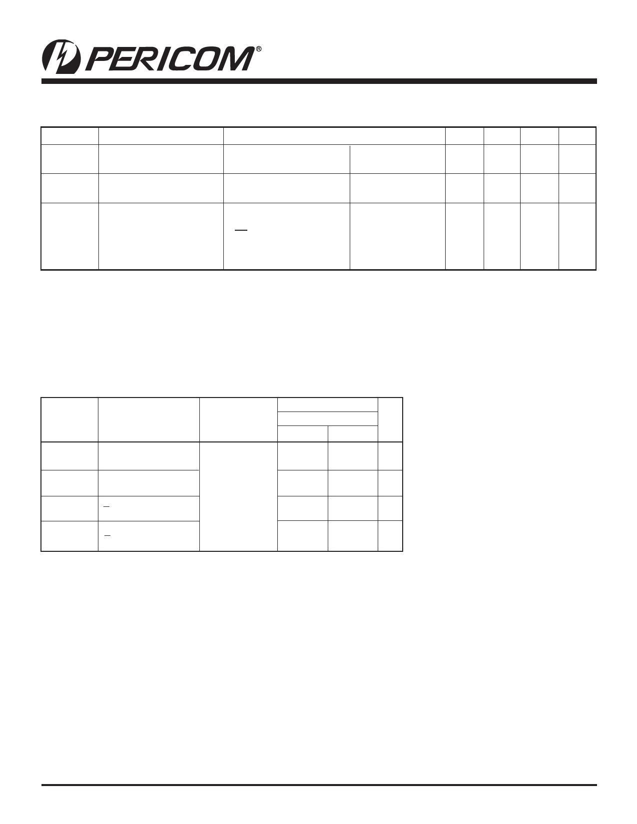
Power Supply Characteristics
Parameters Description
ICC
Quiescent Power
Supply Current
ΔICC
Supply Current per
Input @ TTL HIGH
ICCD
Supply Current per
Input per MHz(4)
Test Conditions(1)
VCC = Max.
VIN = GND or VCC
Min. Typ(2) Max. Units
0.1 3.0 µA
VCC = Max.
VIN = 3.4V(3)
2.5 mA
VCC = Max.,
I and Y Pins Open
BE = GND
Control Input Toggling
50% Duty Cycle
0.25 mA/
MHz
Notes:
1. For Max. or Min. conditions, use appropriate value specified under Electrical Characteristics for the applicable device.
2. Typical values are at Vcc = 5.0V, +25°C ambient.
3. Per TTL driven input (VIN = 3.4V, control inputs only); I and Y pins do not contribute to Icc.
4. This current applies to the control inputs only and represent the current required to switch internal capacitance at the specified
frequency. The I and Y inputs generate no significant AC or DC currents as they transition. This parameter is not tested, but is
guaranteed by design.
Switching Characteristics over Operating Range
Parameters Description
tIY
Propagation Delay(2,3)
In to Yn
tSY
Bus Select Time
Sn to Yn
tPZH
Bus Disable Time
tPZL
E to Yn
tPHZ
Bus Disable Time
tPLZ
E to Yn
Conditions(1)
CL = 50 pF
RL = 500-ohm
PI5C33X257
Com.
Min.
Max. Unit
0.25 ns
0.5
5.2 ns
0.5
4.8 ns
0.5
5.0 ns
Notes:
1. See test circuit and waveforms.
2. This parameter is guaranteed but not tested on Propagation Delays.
3. The bus switch contributes no propagational delay other than the RC delay of the
ON resistance of the switch and the load capacitance. The time constant for the
switch alone is of the order of 0.25ns for 50pF load. Since this time constant is
much smaller than the rise/fall times of typical driving signals, it adds very little
propagational delay to the system. Propagational delay of the bus switch when used
in a system is determined by the driving circuit on the driving side of the switch and
its interaction with the load on the driven side.
06-0237
3
PS8114C 11/03/06
Share Link: 