AD6426 Просмотр технического описания (PDF) - Analog Devices
Номер в каталоге
Компоненты Описание
Список матч
AD6426 Datasheet PDF : 50 Pages
| |||
Preliminary Technical Information
REGISTERS
The AD6426 contains 88 Channel Codec Control Registers, 69
H8 Peripheral Registers mapped into the Channel Codec
address space starting at 8000h. All registers are normally
accessed by the Layer 1 software provided with the
AD20msp425 chipset. The user is not expected to read or
write to any registers other than through the Layer 1 software.
Therefore only a limited description of these registers is given
here to ease the understanding of the functional behavior of
the AD6426. Only registers which can be modified or
monitored by the user under control of the Layer 1 software
are shown. The Channel Codec Control Registers are listed in
Table 1, and the H8 Peripheral Control Registers in Table 3
A description of the Channel Codec Control Register contents
is shown in Table 2, and of the H8 Peripheral Registers in
Table 4.
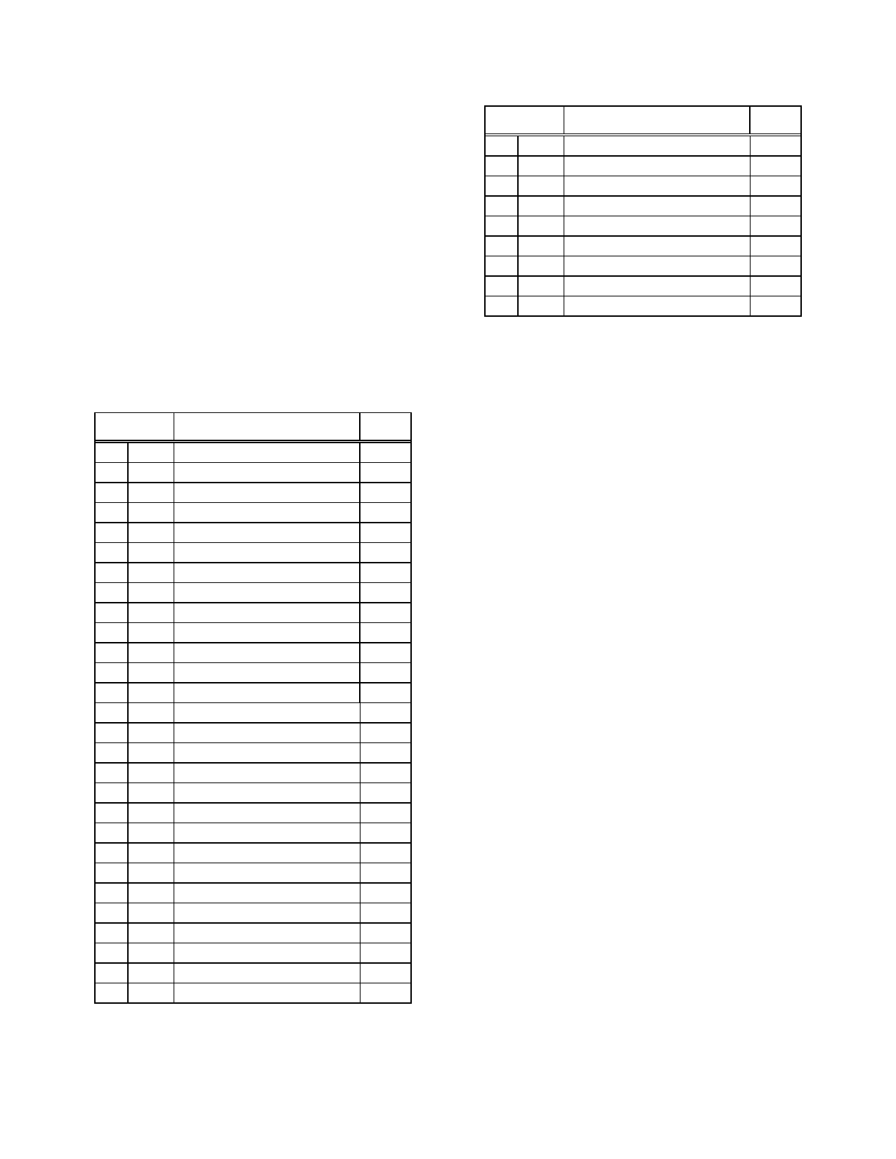
Table 1. CC Control Registers
Address
0 00 H
2 02 H
4 04 H
5 05 H
6 06 H
7 07 H
8 08 H
9 09 H
10 0A H
28 1C H
29 1D H
30 1E H
35 23 H
37 25 H
38 26 H
39 27 H
40 28 H
41 29 H
42 2A H
43 2B H
44 2C H
45 2D H
46 2E H
47 2F H
48 30 H
49 31 H
50 32 H
51 33 H
Name
SYSTEM
RADIO CONTROL
BSIC
TSC
TRAFFIC MODE
DAI
EEPROM
KEYPAD COLUMN
KEYPAD ROW
EVBC SERIAL 1
EVBC SERIAL 2
EVBC IF CONTROL
RESET
SYNTH BIT COUNT
SYNTH CONTROL
ERROR COUNT
SYNTHESIZER 1
SYNTHESIZER 2
SYNTHESIZER 3
SYNTHESIZER 4
POWER CONTROL INT
POWER CONTROL EXTERNAL
SWRESET 1
SWRESET 2
INTERRUPT COUNTER
BBC TX ADDRESS
BACKLIGHT
VERSION CONTROL
R/W
R/W
R/W
R/W
R/W
R/W
R/W
R/W
RD
RMW
RMW
R/W
R/W
R/W
R/W
RMW
WR
WR
WR
WR
R/W
R/W
R/W
R/W
R/W
R/W
WR
RD
AD6426
Address
72 48 H
73 49 H
74 4A H
75 4B H
76 4C H
77 4D H
78 4E H
79 4F H
88 58 H
Name
SYNTHESIZER PROGRAM
TXPA OFFSET 1
TXPA OFFSET 2
TXPA WIDTH 1
TXPA WIDTH 2
IRQ ENABLE
IRQ LATCH
CC GPIO
ccGPO
R/W
R/W
R/W
R/W
R/W
R/W
RMW
R/W
R/W
This Information applies to a product under development. Its characteristics and specifications are subject to change without notice. Analog Devices assumes no
obligation regarding future manufacture unless otherwise agreed to in writing. No responsibility is assumed by Analog Devices for its use; nor for any
infringements of patents or other rights of third parties which may result from its use. No license is granted by implication or otherwise under any patent or patent
rights of Analog Devices.
Revision Preliminary 2.3 (June 9, ´98)
-9-
Confidential Information
Share Link: 