7C132-25 Просмотр технического описания (PDF) - Cypress Semiconductor
Номер в каталоге
Компоненты Описание
Список матч
7C132-25 Datasheet PDF : 18 Pages
| |||
CY7C132/CY7C136
CY7C142/CY7C146
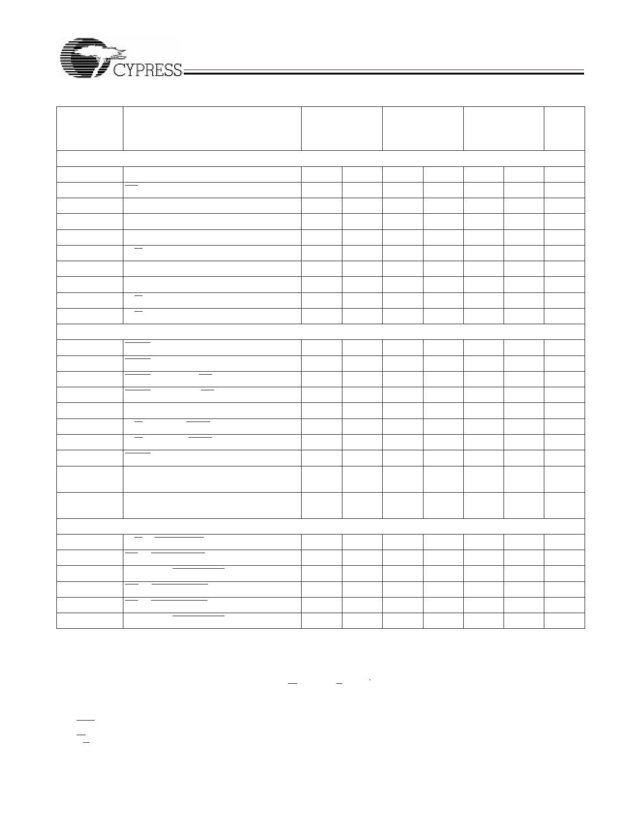
Switching Characteristics Over the Operating Range[6, 11] (continued)
WRITE CYCLE[15]
7C132-35
7C136-35
7C142-35
7C146-35
7C132-45
7C136-45
7C142-45
7C146-45
7C132-55
7C136-55
7C142-55
7C146-55
tWC
Write Cycle Time
tSCE
CE LOW to Write End
tAW
Address Set-Up to Write End
tHA
Address Hold from Write End
tSA
Address Set-Up to Write Start
tPWE
R/W Pulse Width
tSD
Data Set-Up to Write End
tHD
tHZWE
tLZWE
Data Hold from Write End
R/W LOW to High Z [10]
R/W HIGH to Low Z [10]
BUSY/INTERRUPT TIMING
35
45
55
ns
30
35
40
ns
30
35
40
ns
2
2
2
ns
0
0
0
ns
25
30
30
ns
15
20
20
ns
0
0
0
ns
20
20
25
ns
0
0
0
ns
tBLA
tBHA
tBLC
tBHC
tPS
tWB
tWH
tBDD
tDDD
BUSY LOW from Address Match
20
25
30
ns
BUSY HIGH from Address Mismatch[16]
20
25
30
ns
BUSY LOW from CE LOW
BUSY HIGH from CE HIGH[16]
20
25
30
ns
20
25
30
ns
Port Set Up for Priority
5
5
5
ns
R/W LOW after BUSY LOW[17]
0
0
0
ns
R/W HIGH after BUSY HIGH
30
35
35
ns
BUSY HIGH to Valid Data
35
45
45
ns
Write Data Valid to Read Data Valid
Note
18
Note
18
Note
ns
18
tWDD
Write Pulse to Data Delay
INTERRUPT TIMING[19]
Note
18
Note
18
Note
ns
18
tWINS
R/W to INTERRUPT Set Time
25
35
45
ns
tEINS
CE to INTERRUPT Set Time
25
35
45
ns
tINS
tOINR
tEINR
tINR
Address to INTERRUPT Set Time
OE to INTERRUPT Reset Time[16]
CE to INTERRUPT Reset Time[16]
Address to INTERRUPT Reset Time[16]
25
35
45
ns
25
35
45
ns
25
35
45
ns
25
35
45
ns
Notes:
11. Test conditions assume signal transition times of 5 ns or less, timing reference levels of 1.5V, input pulse levels of 0 to 3.0V and output loading of the specified
IOL/IOH, and 30-pF load capacitance.
12. AC test conditions use VOH = 1.6V and VOL = 1.4V.
13. At any given temperature and voltage condition for any given device, tHZCE is less than tLZCE and tHZOE is less than tLZOE.
14. tLZCE, tLZWE, tHZOE, tLZOE, tHZCE, and tHZWE are tested with CL = 5pF as in part (b) of AC Test Loads. Transition is measured ±500 mV from steady-state voltage.
15. The internal write time of the memory is defined by the overlap of CE LOW and R/W LOW. Both signals must be LOW to initiate a write and either signal can terminate
a write by going HIGH. The data input setup and hold timing should be referenced to the rising edge of the signal that terminates the write.
16. These parameters are measured from the input signal changing, until the output pin goes to a high-impedance state.
17. CY7C142/CY7C146 only.
18. A write operation on Port A, where Port A has priority, leaves the data on Port B’s outputs undisturbed until one access time after one of the following:
BUSY on Port B goes HIGH.
Port B’s address toggled.
CE for Port B is toggled.
R/W for Port B is toggled during valid read.
19. 52-pin PLCC and PQFP versions only.
6
Share Link: 