74VHC257 Просмотр технического описания (PDF) - STMicroelectronics
Номер в каталоге
Компоненты Описание
Список матч
74VHC257 Datasheet PDF : 9 Pages
| |||
74VHC257
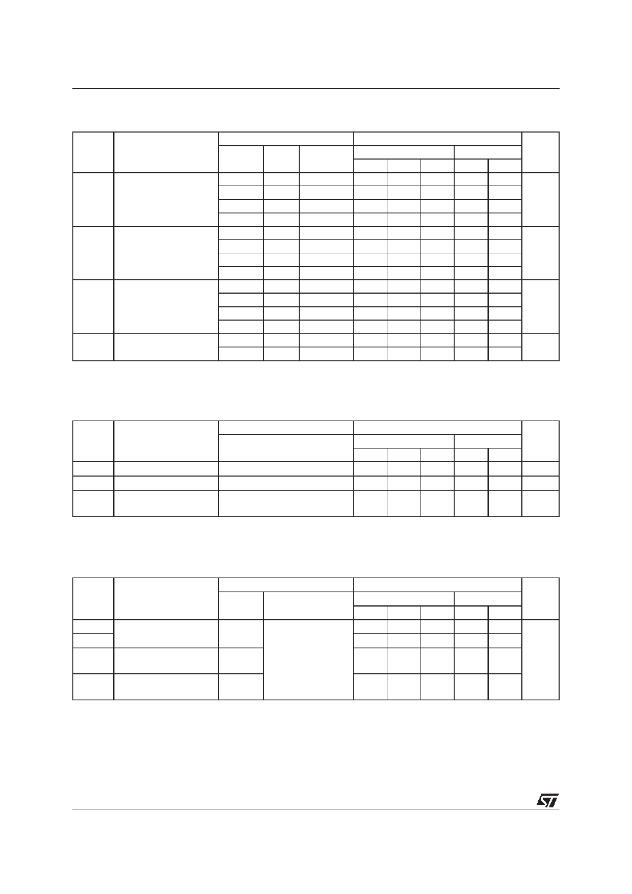
AC ELECTRICAL CHARACTERISTICS (Input tr = tf =3 ns)
Symb ol
Parameter
tPLH Propagation Delay
tPHL Time
A, B to Y
tPLH Propagation Delay
tPHL Time
SELECT to Y
tPZL Output Enable Time
tPZH
tPLZ Output Disable Time
tPHZ
(*) Voltage range is 3.3V ± 0.3V
(**) Voltage range is 5V ± 0.5V
Test Condition
V CC
CL
( V)
(pF)
3.3(*)
15
3.3(*)
50
5.0(**)
15
5.0(**)
50
3.3(*)
15
3.3(*)
50
5.0(**)
15
5.0(**)
50
3.3(*)
15
3.3(*)
50
5.0(**)
15
5.0(**)
50
3.3(*)
50
5.0(**)
50
Value
TA = 25 oC
Min. Typ. Max.
5.8 9.3
8.3 12.8
3.6 5.9
5.1 7.9
7.0 11.0
9.5 14.5
4.0 6.8
5.5 8.8
6.7 10.5
9.2 14.0
3.6 6.8
5.1 8.8
8.6 12.0
5.7 7.9
-40 to 85 oC
Min . Max.
1.0 11.0
1.0 14.5
1.0 7.0
1.0 9.0
1.0 13.0
1.0 16.5
1.0 8.0
1.0 10.0
1.0 12.5
1.0 16.0
1.0 8.0
1.0 10.0
1.0 13.5
1.0 9.0
Unit
ns
ns
ns
ns
CAPACITIVE CHARACTERISTICS
Symb ol
Parameter
Test Conditions
Value
Un it
TA = 25 oC
-40 to 85 oC
Min. Typ . Max. Min . Max.
CIN Input Capacitance
4
10
10
pF
COUT Output Capacitance
6
pF
CPD Power Dissipation
Capacitance (note 1)
23
pF
1) CPD isdefined as the value of the IC’sinternal equivalent capacitance which is calculated fromthe operating current consumption without load. (Referto
Test Circuit).Average operating current can be obtained by the following equation. ICC(opr) = CPD • VCC • fIN + ICC/4 (per Channel)
DYNAMIC SWITCHING CHARACTERISTICS
Symb ol
Parameter
Test Conditions
V CC
( V)
Value
TA = 25 oC
Min. Typ. Max.
-40 to 85 oC
Min . Max.
Un it
VOLP Dynamic Low Voltage
5.0
VOLV Quiet Output (note 1, 2)
0.3 0.8
-0.8 -0.3
VIHD Dynamic High Voltage
5.0
CL = 50 pF
3.5
V
Input (note 1, 3)
VILD Dynamic Low Voltage
5.0
1.5
Input (note 1, 3)
1) Worst case package.
2) Max number of outputs defined as (n). Data inputs are driven 0V to 5.0V, (n -1) outputs switching and one output at GND.
3) Max number of data inputs (n) switching. (n-1) switching 0V to5.0V. Inputs under test switching: 5.0V to threshold (VILD), 0V to threshold (VIHD), f=1MHz.
4/9
Share Link: 