74LVT574WM Просмотр технического описания (PDF) - Fairchild Semiconductor
Номер в каталоге
Компоненты Описание
Список матч
74LVT574WM Datasheet PDF : 8 Pages
| |||
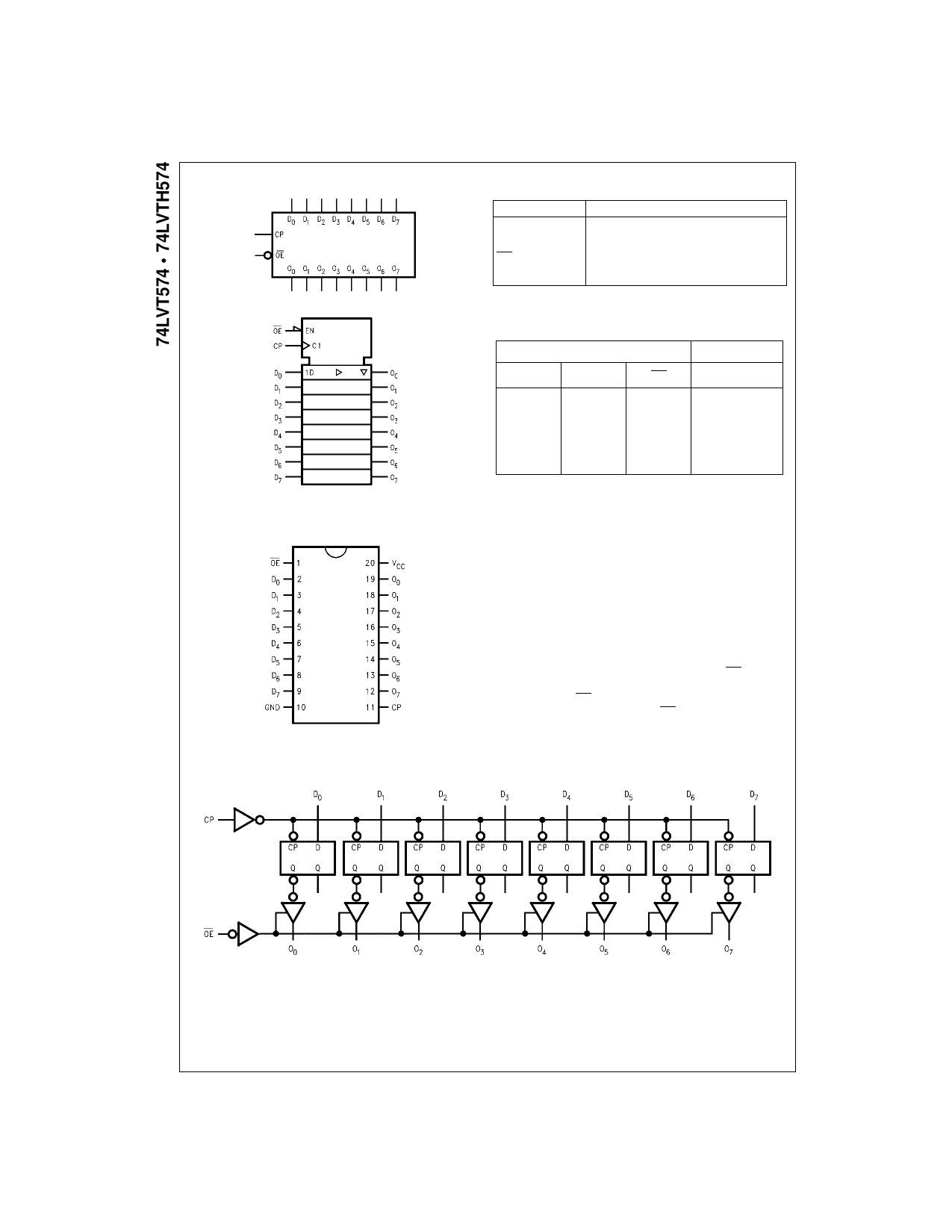
Logic Symbols
IEEE/IEC
Connection Diagram
Logic Diagram
Pin Descriptions
Pin Names
D0–D7
CP
OE
O0–O7
Description
Data Inputs
Clock Pulse Input
3-STATE Output Enable Input
3-STATE Outputs
Truth Table
Inputs
Dn
H
CP
OE
L
L
L
X
L
L
X
X
H
H HIGH Voltage Level
L LOW Voltage Level
X Immaterial
Z High Impedance
LOW-to-HIGH Transition
Oo Previous Oo before HIGH to LOW of CP
Outputs
On
H
L
Oo
Z
Functional Description
The LVT574 and LVTH574 consist of eight edge-triggered
flip-flops with individual D-type inputs and 3-STATE true
outputs. The buffered clock and buffered Output Enable
are common to all flip-flops. The eight flip-flops will store
the state of their individual D-type inputs that meet the
setup and hold time requirements on the LOW-to-HIGH
Clock (CP) transition. With the Output Enable (OE) LOW,
the contents of the eight flip-flops are available at the out-
puts. When the OE is HIGH, the outputs go to the high
impedance state. Operation of the OE input does not affect
the state of the flip-flops.
Please note that this diagram is provided only for the understanding of logic operations and should not be used to estimate propagation delays.
www.fairchildsemi.com
2
Share Link: 