74HCT75 Просмотр технического описания (PDF) - Philips Electronics
Номер в каталоге
Компоненты Описание
Список матч
74HCT75 Datasheet PDF : 7 Pages
| |||
Philips Semiconductors
Quad bistable transparent latch
Product specification
74HC/HCT75
FEATURES
• Complementary Q and Q outputs
• VCC and GND on the centre pins
• Output capability: standard
• ICC category: MSI
GENERAL DESCRIPTION
The 74HC/HCT75 are high-speed Si-gate CMOS devices
and are pin compatible with low power Schottky TTL
(LSTTL). They are specified in compliance with JEDEC
standard no. 7A.
The 74HC/HCT75 have four bistable latches. The two
latches are simultaneously controlled by one of two active
HIGH enable inputs (LE1-2 and LE3-4). When LEn-n is
HIGH, the data enters the latches and appears at the nQ
outputs. The nQ outputs follow the data inputs (nD) as long
as LEn-n is HIGH (transparent). The data on the nD inputs
one set-up time prior to the HIGH-to-LOW transition of the
LEn-n will be stored in the latches. The latched outputs
remain stable as long as the LEn-n is LOW.
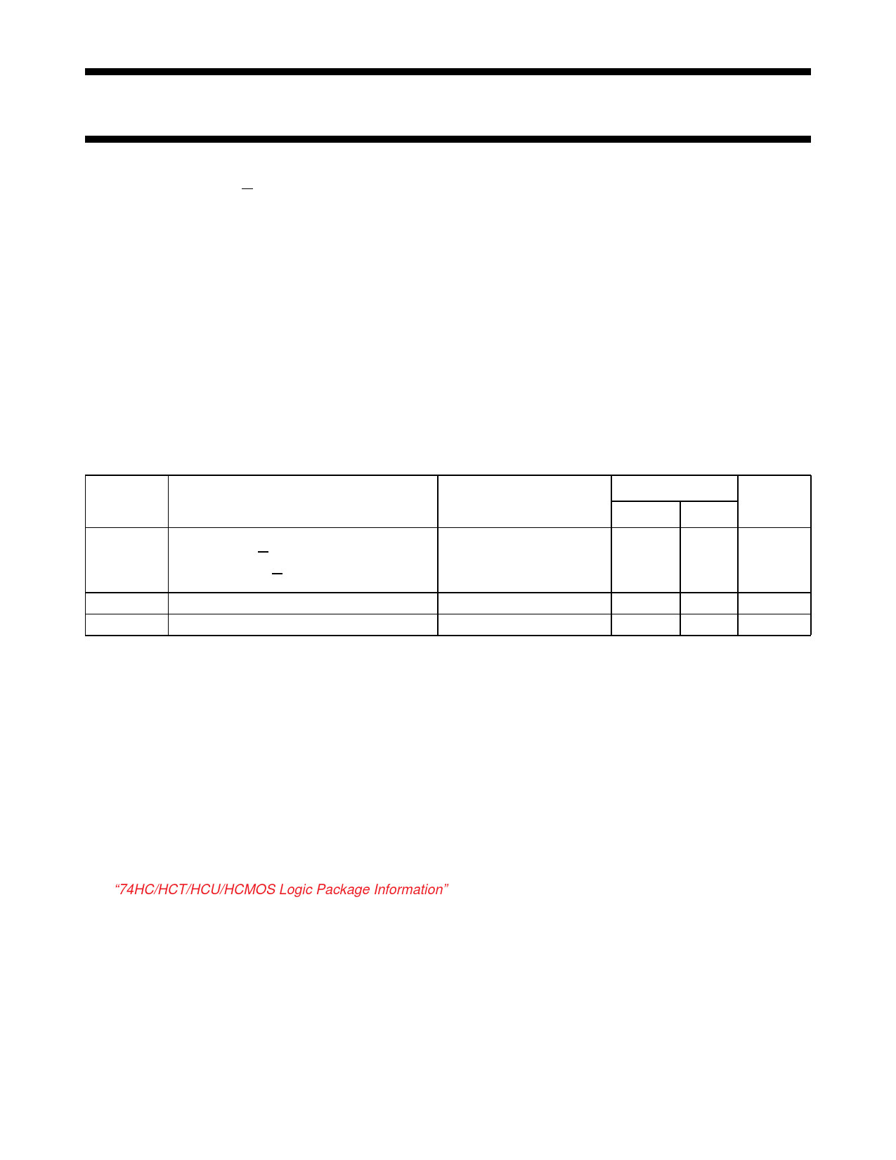
QUICK REFERENCE DATA
GND = 0 V; Tamb = 25 °C; tr = tf = 6 ns
SYMBOL
PARAMETER
CONDITIONS
tPHL/ tPLH
CI
CPD
propagation delay
nD to nQ, nQ
LEn-n to nQ, nQ
input capacitance
power dissipation capacitance per latch
CL = 15 pF; VCC = 5 V
notes 1 and 2
Notes
1. CPD is used to determine the dynamic power dissipation (PD in µW):
PD = CPD × VCC2 × fi + ∑ (CL × VCC2 × fo) where:
fi = input frequency in MHz
fo = output frequency in MHz
∑ (CL × VCC2 × fo) = sum of outputs
CL = output load capacitance in pF
VCC = supply voltage in V
2. For HC the condition is VI = GND to VCC
For HCT the condition is VI = GND to VCC −1.5 V
ORDERING INFORMATION
See “74HC/HCT/HCU/HCMOS Logic Package Information”.
TYPICAL
HC
HCT
UNIT
11
12
ns
11
11
ns
3.5
3.5
pF
42
42
pF
December 1990
2
Share Link: 