74ACTQ652 Просмотр технического описания (PDF) - Fairchild Semiconductor
Номер в каталоге
Компоненты Описание
Список матч
74ACTQ652 Datasheet PDF : 9 Pages
| |||
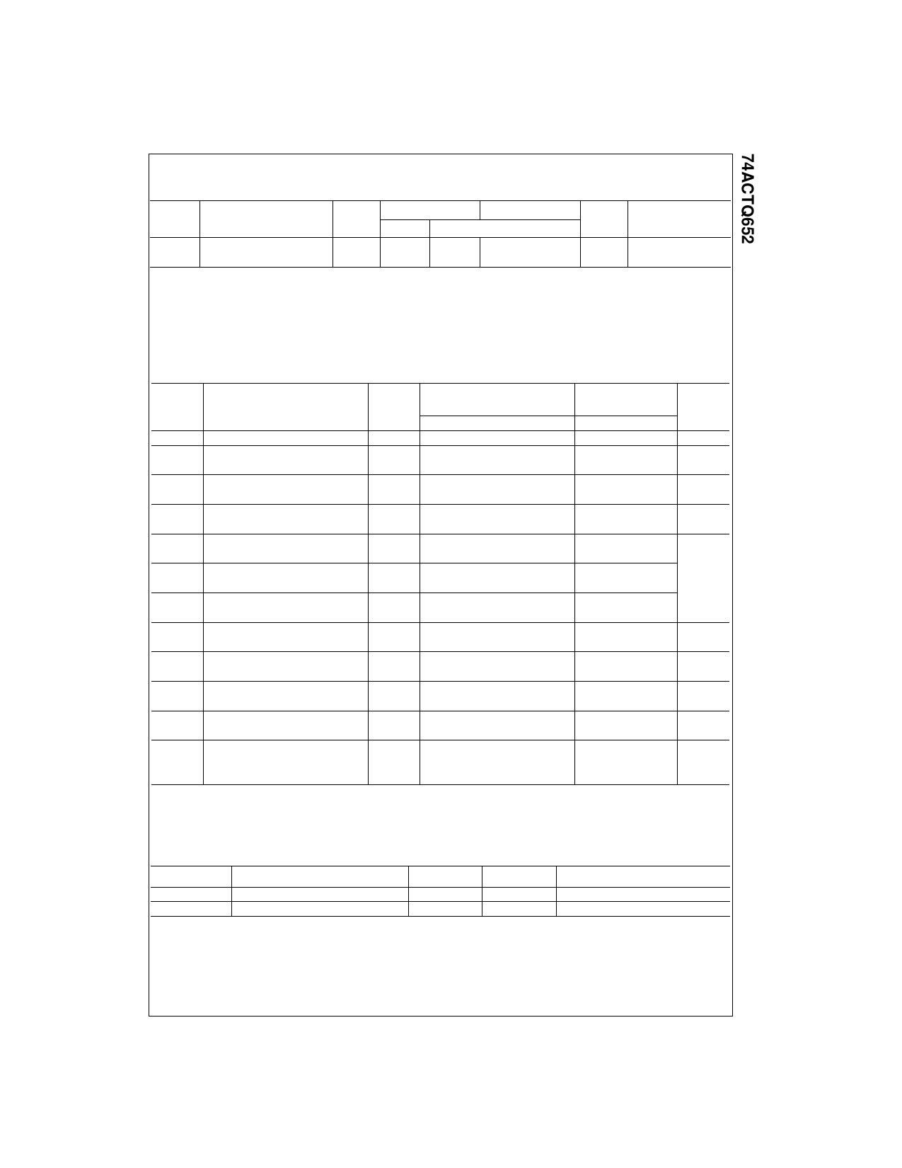
DC Electrical Characteristics (Continued)
Symbol
Parameter
VCC
TA = +25°C
TA = −40°C to +85°C
Units
(V)
Typ
Guaranteed Limits
Conditions
VILD
Maximum LOW Level
Dynamic Input Voltage
5.0
1.2
0.8
V
(Note 5)(Note 7)
Note 3: All outputs loaded; thresholds on input associated with output under test.
Note 4: Maximum test duration 2.0 ms, one output loaded at a time.
Note 5: PDIP package.
Note 6: Max number of outputs defined as (n). Data inputs are driven 0V to 3V. One output @ GND.
Note 7: Max number of data inputs (n) switching. (n − 1) inputs switching 0V to 3V (ACTQ). Input-under-test switching: 3V to threshold (VILD),
0V to threshold (VIHD), f = 1 MHz.
AC Electrical Characteristics
VCC
TA = +25°C
TA = −40°C to +85°C
Symbol
Parameter
(V)
CL = 50 pF
CL = 50 pF
Units
(Note 8)
Min
Typ
Max
Min
Max
fMAX
tPLH
tPHL
tPLH
tPHL
tPLH
tPHL
tPZH
tPZL
tPHZ
tPLZ
tPZH
tPZL
tPHZ
tPLZ
ts(H)
ts(L)
th(H)
th(L)
tw(H)
tw(L)
tOSHL
tOSLH
Maximum Clock Frequency
Propagation Delay
Clock to Bus
Propagation Delay
Bus to Bus
Propagation Delay
SBA or SAB to A or B
Enable Time
OEBA to A (Note 8)
Disable Time
OEBA to A (Note 8)
Enable Time
OEAB to B
Disable Time
OEAB to B
Setup Time, HIGH or
LOW, Bus to Clock
Hold Time, HIGH or
LOW, Bus to Clock
Clock Pulse Width
HIGH or LOW
Output to Output Skew (Note 9)
A to B, B to A or
Clock to Output
5.0
MHz
5.0
2.0
7.0
9.5
2.0
10.0
ns
5.0
2.0
6.5
9.0
2.0
9.5
ns
5.0
2.5
6.5
10.0
2.5
10.5
ns
5.0
2.0
7.0
10.5
2.0
11.0
5.0
1.0
5.0
8.0
1.0
8.5
ns
5.0
2.0
7.0
10.5
2.0
11.0
5.0
1.0
5.0
8.0
1.0
8.5
ns
5.0
3.0
3.0
ns
5.0
1.5
1.5
ns
5.0
4.0
4.0
ns
5.0
0.5
1.0
1.0
ns
Note 8: Voltage Range 5.0 is 5.0V ± 0.5V.
Note 9: Skew is defined as the absolute value of the difference between the actual propagation delay for any separate outputs of the same device. The spec-
ification applies to any output switching in the same direction, either HIGH-to-LOW (TOSHL) or LOW-to-HIGH (TOSLH). Parameter guaranteed by design.
Capacitance
Symbol
CIN
CPD
Parameter
Input Capacitance
Power Dissipation Capacitance
Typ
Units
Conditions
4.5
pF
VCC = 5.0V
54
pF
VCC = 5.0V
5
www.fairchildsemi.com
Share Link: 