74ABT534A Просмотр технического описания (PDF) - Philips Electronics
Номер в каталоге
Компоненты Описание
Список матч
74ABT534A Datasheet PDF : 12 Pages
| |||
Philips Semiconductors
Octal D-type flip-flop, inverting (3-State)
Product specification
74ABT534A
FEATURES
• 8-bit positive edge triggered register
• 3-State output buffers
• Output capability: +64mA/–32mA
• Latch-up protection exceeds 500mA per Jedec JC40.2 Std 17
• ESD protection exceeds 2000 V per MIL STD 883 Method 3015
and 200 V per Machine Model
• Power-up 3-State
DESCRIPTION
The 74ABT534A high-performance BiCMOS device combines low
static and dynamic power dissipation with high speed and high
output drive.
The 74ABT534A is an 8-bit, edge triggered register coupled to eight
3-State output buffers. The two sections of the device are controlled
independently by the clock (CP) and Output Enable (OE) control
gates.
The register is fully edge triggered. The state of each D input, one
set-up time before the Low-to-High clock transition, is transferred to
the corresponding flip-flop’s output.
The 3-State output buffers are designed to drive heavily loaded
3-State buses, MOS memories, or MOS microprocessors. The
active-Low Output Enable (OE) controls all eight 3-State buffers
independent of the clock operation.
QUICK REFERENCE DATA
When OE is Low, the stored data appears at the outputs. When OE
is High, the outputs are in the High-impedance “OFF” state, which
means they will neither drive nor load the bus.
SYMBOL
tPLH
tPHL
CIN
PARAMETER
Propagation delay
CP to Qn
Input capacitance
CONDITIONS
Tamb = 25°C; GND = 0V
CL = 50pF; VCC = 5V
VI = 0V or VCC
TYPICAL
3.3
3.6
3.5
UNIT
ns
pF
COUT
ICCZ
Output capacitance
Total supply current
Outputs disabled; VO = 0V or VCC
Outputs disabled; VCC =5.5V
6.5
pF
100
µA
ORDERING INFORMATION
PACKAGES
20-Pin Plastic DIP
20-Pin plastic SO
20-Pin Plastic SSOP Type II
20-Pin Plastic TSSOP Type I
TEMPERATURE RANGE OUTSIDE NORTH AMERICA
–40°C to +85°C
74ABT534A N
–40°C to +85°C
74ABT534A D
–40°C to +85°C
74ABT534A DB
–40°C to +85°C
74ABT534A PW
NORTH AMERICA
74ABT534A N
74ABT534A D
74ABT534A DB
74ABT534APW DH
DWG NUMBER
SOT146-1
SOT163-1
SOT339-1
SOT360-1
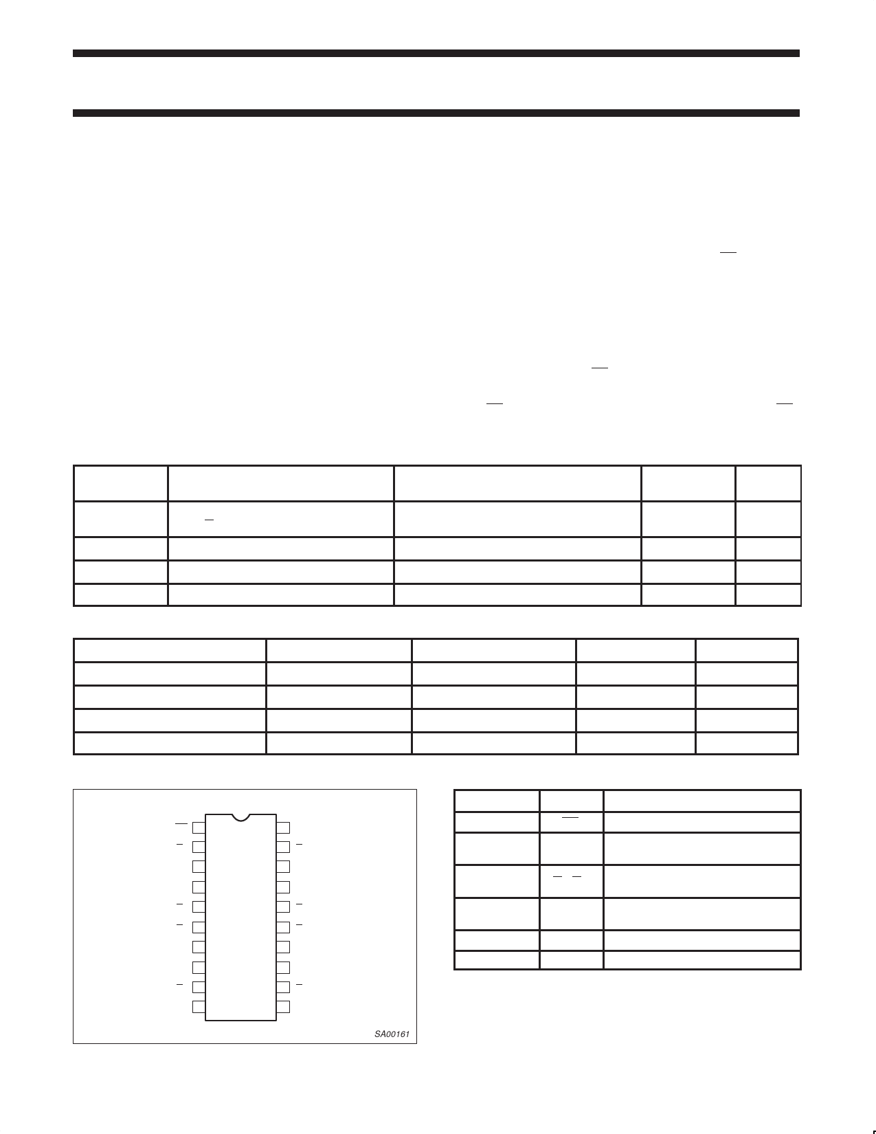
PIN CONFIGURATION
OE 1
Q0 2
D0 3
D1 4
Q1 5
Q2 6
D2 7
D3 8
Q3 9
GND 10
20 VCC
19 Q7
18 D7
17 D6
16 Q6
15 Q5
14 D5
13 D4
12 Q4
11 CP
PIN DESCRIPTION
PIN NUMBER SYMBOL
FUNCTION
1
OE Output enable input (active-Low)
3, 4, 7, 8,
13, 14, 17, 18
2, 5, 6, 9,
12, 15, 16, 19
D0-D7 Data inputs
Q0-Q7 Inverting 3-State outputs
11
CP
Clock pulse input
(active rising edge)
10
GND Ground (0V)
20
VCC Positive supply voltage
SA00161
1997 Feb 03
2
853-1910 17722
Share Link: 