74ABT16260(2002) Просмотр технического описания (PDF) - Philips Electronics
Номер в каталоге
Компоненты Описание
Список матч
74ABT16260 Datasheet PDF : 12 Pages
| |||
Philips Semiconductors
12-bit to 24-bit multiplexed D-type latch (3-State)
Product data
74ABT16260
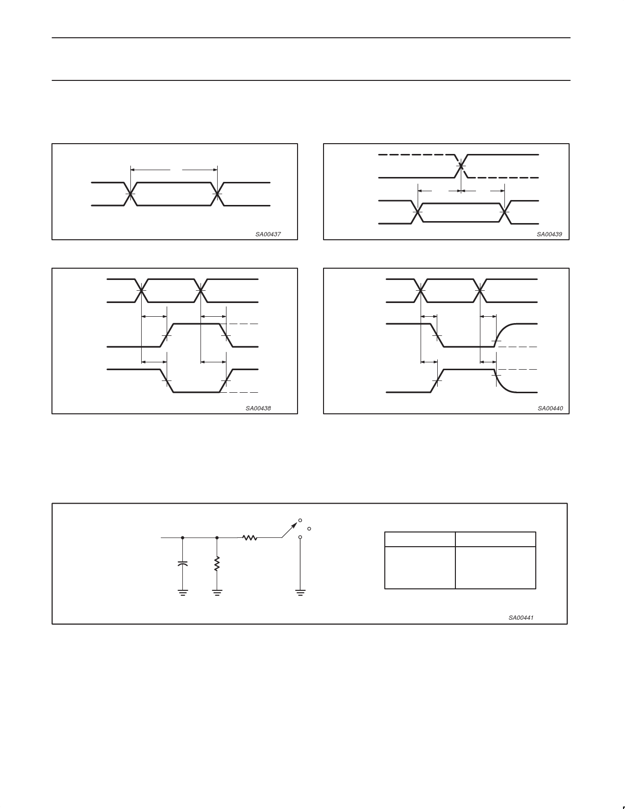
AC WAVEFORMS
VM = 1.5 V for all waveforms
The outputs are measured one at a time with one transition per measurement.
INPUT
tw
VM
3V
VM
0V
Figure 1. Pulse duration
SA00437
TIMING INPUT
DATA INPUT
VM
tsu
VM
th
VM
Figure 3. Set-up and hold times
3V
0V
3V
0V
SA00439
INPUT
OUTPUT
OUTPUT
VM
tPLH
VM
tPHL
VM
VM
tPHL
VM
tPLH
VM
3V
0V
VOH
VOL
VOH
VOL
SA00438
All input pulses are supplied by generators having the following
characteristics: PRR ≤ 10 MHz, ZO = 50 Ω, tr ≤ 2.5 ns, tf ≤ 2.5 ns.
Figure 2. Propagation delay times;
inverting and non-inverting outputs
TEST LOAD CIRCUIT
FROM OUTPUT UNDER TEST
CL = 50 pF
(INCLUDES PROBE AND
JIG CAPACITANCE)
500 Ω
S1
500 Ω
OUTPUT
CONTROL
OUTPUT
WAVEFORM 1
S1 AT 7V
OUTPUT
WAVEFORM 2
S1 AT OPEN
VM
tPZL
VM
tPZH
VM
VM
tPLZ
3V
0V
3.5V
tPHZ
VOL + 0.3V
VOL
VOH
VOH – 0.3V
≈0V
SA00440
Waveform 1 is for an output with internal conditions such that the
output is LOW except when disabled by the output control.
Waveform 2 is for an output with internal conditions such that the
output is HIGH except when disabled by the output control.
Figure 4. Enable and disable times;
LOW- and HIGH-level enabling
7V
OPEN
GND
TEST
tPLH/tPHL
tPLZ/tPZL
tPHZ/tPZH
S1
Open
7V
Open
Load Circuit for Outputs
Figure 5. Test load circuit
SA00441
2002 Apr 03
8
Share Link: 