604DCR100(2013) Просмотр технического описания (PDF) - Naina Semiconductor ltd.
Номер в каталоге
Компоненты Описание
Список матч
604DCR100 Datasheet PDF : 3 Pages
| |||
Naina Semiconductor Ltd.
Blocking Parameters (TJ = 25oC, unless otherwise specified)
Parameters
Critical rate of rise of off-state voltage @ TJ = TJ max, linear to 80% rated
VDRM
Maxmimum peak reverse & off-state leakage current @ TJ = TJ max, rated
VDRM/VRRM applied
Symbol
dV/dt
IRRM, IDRM
Triggering Parameters (TJ = 25oC, unless otherwise specified)
Parameters
DC gate current to trigger
DC gate voltage to trigger
Symbol
IGT
VGT
Thermal and Mechanical Specifications (TJ = 25oC, unless otherwise specified)
Parameters
Symbol
Maximum operating junction temperature range
TJ
Maximum storage temperature range
TStg
Maximum thermal resistance, junction to case
Rth(JC)
Mounting torque
F
Approximate weight
WT
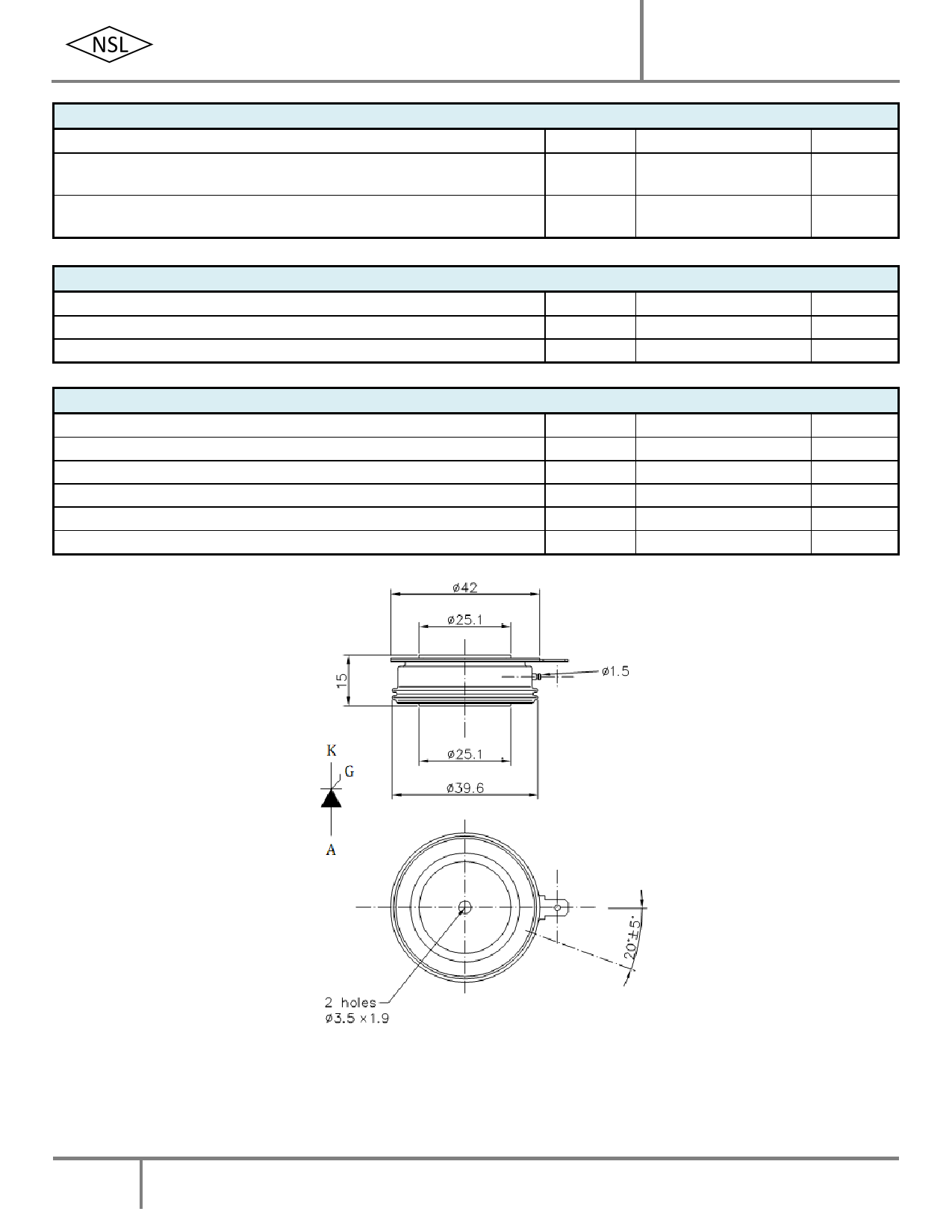
Package Outline
604DCR
Values
500
40
Units
V/µs
mA
Values
200
3.0
Values
- 40 to +125
- 40 to +125
0.06
9 … 11
90
Units
mA
V
Units
oC
oC
oC/W
kN
g
ALL DIMENSIONS IN MM
2
D-95, Sector 63, Noida – 201301, India • Tel: 0120-4205450 • Fax: 0120-4273653
sales@nainasemi.com • www.nainasemi.com
Share Link: 