5962R9582401QQC(1996) Просмотр технического описания (PDF) - Intersil
Номер в каталоге
Компоненты Описание
Список матч
5962R9582401QQC Datasheet PDF : 19 Pages
| |||
HS-80C85RH
Functional Description
The HS-80C85RH is a complete 8-bit parallel central pro-
cessing unit implemented in a self aligned, silicon gate,
CMOS technology. Its static design allows the device to be
operated at any external clock frequency from a maximum of
4MHz down to DC. The processor clock can be stopped in
either the high or low state and held there indefinitely. This
type of operation is especially useful for system debug or
power critical applications. The device is designed to fit into
a minimum system of three ICs: CPU (HS-80C85RH), RAM/
IO (HS-81C55/56RH) and ROM/IO Chip (HS-83C55RH).
Since the HS-80C85RH is implemented in CMOS, all of the
advantages of CMOS technology are inherent in the device.
These advantages include low standby and operating power,
high noise immunity, moderately high speed, wide operating
temperature range, and designed-in radiation hardness.
Thus the HS-80C85RH is ideal for weapons and space
applications.
The HS-80C85RH has twelve addressable 8-bit registers.
Four of them can function only as two 16-bit register pairs.
Six others can be used interchangeably as 8-bit registers or
as 16-bit register pairs. The HS-80C85RH register set is as
follows:
enabled or disabled by El or Dl software instructions), and
causes the CPU to fetch in an RST instruction, externally
placed on the data bus, which vectors a branch to any one of
eight fixed memory locations (Restart addresses). The deci-
mal addresses of these dedicated locations are: 0, 8, 16,
24, 32, 40, 48, and 56. Any of these addresses may be used
to store the first instruction(s) of a routine designed to
service the requirements of an interrupting device. Since the
(RST) is a call, completion of the instruction also stores the
old program counter contents on the STACK. Each of the
three RESTART inputs, 5.5, 6.5, and 7.5, has a programma-
ble mask. TRAP is also a RESTART interrupt but it is
nonmaskable.
The three maskable interrupts cause the internal execution
of RESTART (saving the program counter in the stack and
branching to the RESTART address) if the interrupts are
enabled and if the interrupt mask is not set. The non-
maskable TRAP causes the internal execution of a
RESTART vector independent of the state of the interrupt
enable or masks. (See Table 9.)
There are two different types of inputs in the restart
interrupts. RST 5.5 and RST 6.5 are high level-sensitive and
are recognized with the same timing as INTR. RST 7.5 is
rising edge sensitive.
MNEMONIC
ACC or A
PC
BC, DE, HL
SP
Flags or F
REGISTER
Accumulator
Program Counter
General-Purpose
Registers; Data
Pointer(HL)
Stack Pointer
Flag Register
CONTENTS
8 -bits
16-bit Address
8-bits x 6 or
16-bits x 3
16-bit Address
5 Flags (8-bit space)
For RST 7.5, only a pulse is required to set an internal
flipflop which generates the internal interrupt request (a
normally high level signal with a low going pulse is recom-
mended for highest system noise immunity). The RST 7.5
request flip-flop remains set until the request is serviced.
Then it is reset automatically. This flip-flop may also be reset
by using the SlM instruction or by issuing a RESET IN to the
80C85RH. The RST 7.5 internal flip-flop will be set by a
pulse on the RST 7.5 pin even when the RST 7.5 interrupt is
masked out.
The status of the three RST interrupt masks can only be
affected by the SIM instruction and RESET IN.
The HS-80C85RH uses a multiplexed Data Bus. The
address is split between the higher 8-bit Address Bus and
the lower 8-bit Address/Data Bus. During the first T state
(clock cycle) of a machine cycle the low order address is
sent out on the Address/Data bus. These lower 8 bits may
be latched externally by the Address Latch Enable signal
(ALE). During the rest of the machine cycle the data bus is
used for memory or I/O data.
The interrupts are arranged in a fixed priority that determines
which interrupt is to be recognized if more than one is
pending as follows: TRAP-highest priority, RST 7.5, RST
6.5, RST 5.5, INTR-lowest priority. This priority scheme does
not take into account the priority of a routine that was started
by a higher priority interrupt. RST 5.5 can interrupt an RST
7.5 routine if the interrupts are re-enabled before the end of
the RST 7.5 routine.
The HS-80C85RH provides RD, WR, S0, S1, and IO/M sig-
nals for bus control. An Interrupt Acknowledge signal (INTA)
is also provided. HOLD and all Interrupts are synchronized
with the processor’s internal clock. The HS-80C85RH also
provides Serial Input Data (SID) and Serial Output Data
(SOD) lines for simple serial interface.
In addition to these features, the HS-80C85RH has three
maskable, vector interrupt pins, one nonmaskable TRAP
interrupt, and a bus vectored interrupt, INTR.
Interrupt and Serial I/O
The HS-80C85RH has 5 interrupt inputs: INTR, RST 5.5,
RST 6.5, RST 7.5, and TRAP INTR is maskable (can be
The TRAP interrupt is useful for catastrophic events such as
power failure or bus error. The TRAP input is recognized just
as any other interrupt but has the highest priority. It is not
affected by any flag or mask. The TRAP input is both edge
and level sensitive. The TRAP input must go high and
remain high until it is acknowledged. It will not be recognized
again until it goes low, then high again. This avoids any false
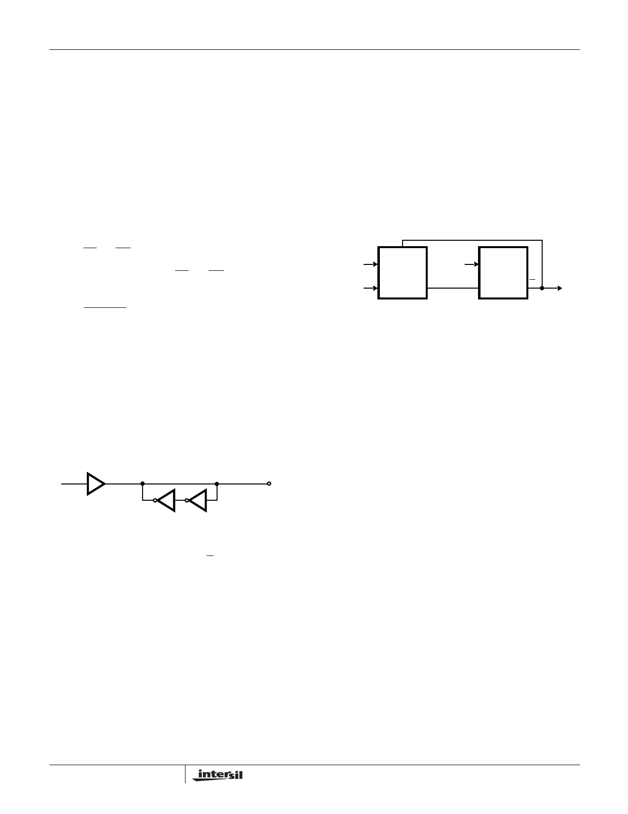
triggering due to noise or logic glitches. Figure 8illustrates
the TRAP interrupt request circuitry within the HS-80C85RH.
Note that the servicing of any interrupt (TRAP, RST 7.5, RST
6.5, RST 5.5, INTR) disables all future interrupts (except
TRAPs) until an EI instruction is executed.
Spec Number 518054
12
Share Link: 