HM628128DLFP-7 Просмотр технического описания (PDF) - Hitachi -> Renesas Electronics
Номер в каталоге
Компоненты Описание
Список матч
HM628128DLFP-7 Datasheet PDF : 20 Pages
| |||
HM628128D Series
Low VCC Data Retention Characteristics (Ta = –20 to +70°C)
Parameter
Symbol Min Typ*5 Max Unit Test conditions*4
VCC for data retention
VDR
2.0 —
—V
Vin ≥ 0V
(1) 0 V ≤ CS2 ≤ 0.2 V or
(2) CS2 ≥ VCC – 0.2 V
CS1 ≥ VCC – 0.2 V
Data retention current
I
*1
CCDR
—
1.0 50
µA
VCC = 3.0 V, Vin ≥ 0 V
(1) 0 V ≤ CS2 ≤ 0.2 V or
(2) CS2 ≥ VCC – 0.2 V,
CS1 ≥ VCC – 0.2 V
I
*2
CCDR
—
1.0
15
µA
I
*3
CCDR
—
0.5
10
µA
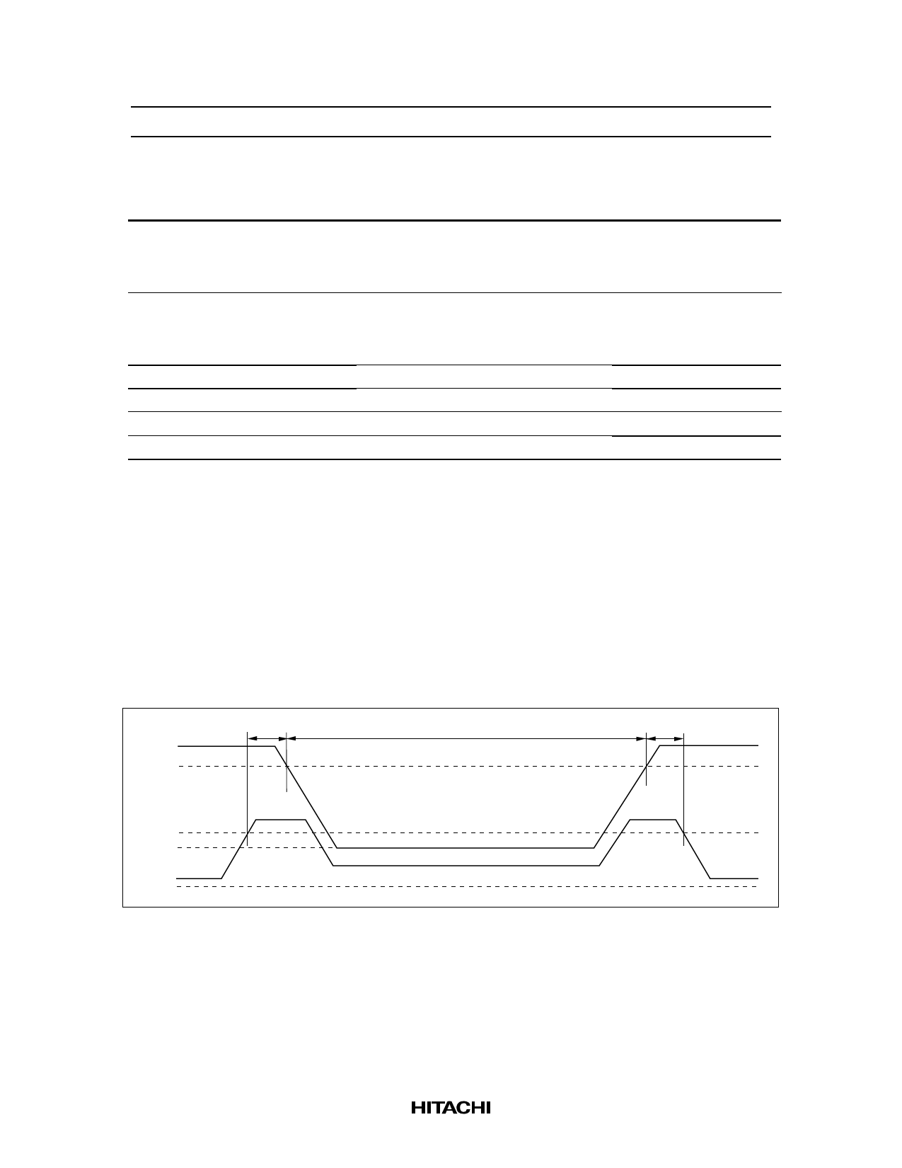
Chip deselect to data retention time tCDR
0
—
— ns
See retention waveform
Operation recovery time
tR
tRC*6 —
— ns
Notes: 1. This characteristic is guaranteed only for L-version, 20 µA max. at Ta = –20 to +40°C.
2. This characteristic is guaranteed only for L-SL-version, 3 µA max. at Ta = –20 to +40°C.
3. This characteristic is guaranteed only for L-UL-version, 1 µA max. at Ta = –20 to +40°C.
4. CS2 controls address buffer, WE buffer, CS1 buffer, OE buffer, and Din buffer. If CS2 controls
data retention mode, Vin levels (address, WE, OE, CS1, I/O) can be in the high impedance state.
If CS1 controls data retention mode, CS2 must be CS2 ≥ VCC – 0.2 V or 0 V ≤ CS2 ≤ 0.2 V. The
other input levels (address, WE, OE, I/O) can be in the high impedance state.
5. Typical values are at VCC = 3.0 V, Ta = +25°C and specified loading, and not guaranteed.
6. tRC = read cycle time.
Low VCC Data Retention Timing Waveform (1) (CS1 Controlled)
tCDR
Data retention mode
tR
VCC
4.5 V
2.2 V
VDR
CS1
0V
CS1 ≥ VCC – 0.2 V
12
Share Link: 