RT9173ACM5 Просмотр технического описания (PDF) - Richtek Technology
Номер в каталоге
Компоненты Описание
Список матч
RT9173ACM5 Datasheet PDF : 10 Pages
| |||
RT9173/A
Applications Information
Internal parasitic diode
Avoid forward-bias internal parasitic diode, VOUT to
VCNTL, and VOUT to VIN, the VOUT should not be
forced some voltage respect to ground on this pin
while the VCNTL or VIN is disappeared.
Consideration while designs the resistance of
voltage divider
Make sure the sinking current capability of pull-down
NMOS if the lower resistance was chosen so that the
voltage on REFEN is below 0.2V.
In addition to item 1, the capacitor and voltage divider
form the low-pass filter. There are two reasons doing
this design; one is for output voltage soft-start while
another is for noise immunity.
How to reduce power dissipation on Notebook PC
or the dual channel DDR SDRAM application?
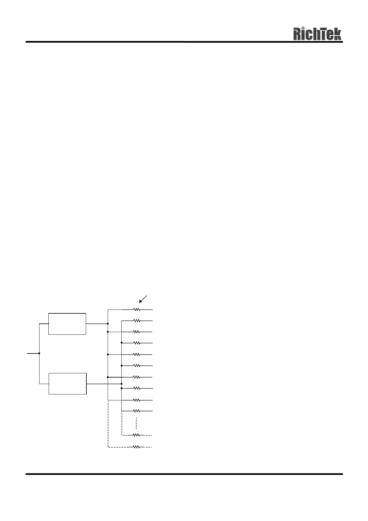
In notebook application, using RichTek’s Patent
“Distributed Bus Terminator Topology” with choosing
RichTek’s product is encouraged.
REFEN
Distributed Bus Terminating Topology
Terminator Resistor
RT9173
VOUT
RT9173
VOUT
R0
BUS(0)
R1
BUS(1)
R2
BUS(2)
R3
BUS(3)
R4
BUS(4)
R5
BUS(5)
R6
BUS(6)
R7
BUS(7)
R8
BUS(8)
R9
BUS(9)
RN
RN 1
BUS(N+1)
BUS(N)
Thermal Consideration
RT9173/A regulators have internal thermal limiting
circuitry designed to protect the device during
overload conditions. For continuous normal load
conditions however, the maximum junction
temperature rating of 125°C must not be exceeded.
Higher continous currents or ambient temperature
require additional heatsinking. Heat sinking to the IC
package must consider the worst case power
dissipation which may occur.
It should also be note that with the VCNTL equal to
5V, the point of thermal shutdown will be degraded by
approx. 20°C compared to the VCNTL equipped with
3.3V. It is highly recommended that to use the 3.3V
rail acted as the VCNTL so as to minimize the
thermal concern of the RT9173CS in the SOP-8
package.
Layout Consideration
The RT9173CS regulator is packaged in plastic SOP-
8 package. This small footprint package is unable to
convectively dissipate the heat generated when the
regulator is operating at high current levels. In order
to control die operating temperatures, the PC board
layout should allow for maximum possible copper
area at the VCNTL pins of the RT9173CS.
The multiple VCNTL pins on the SOP-8 package are
internally connected, but lowest thermal resistance
will result if these pins are tightly connected on the
PC board. This will also aid heat dissipation at high
power levels.
If the large copper around the IC is unavailable, a
buried layer may be used as a heat spreader, Use
vias to conduct the heat into the buried or backside of
PCB layer. The vias should be small enough to retain
solder when the board is wave-soldered. (See Fig.6
shown on next page).
www.richtek-ic.com.tw
6
DS9173/A-06 March 2002
Share Link: 