AD8346 Просмотр технического описания (PDF) - Analog Devices
Номер в каталоге
Компоненты Описание
Список матч
AD8346 Datasheet PDF : 20 Pages
| |||

AD8346
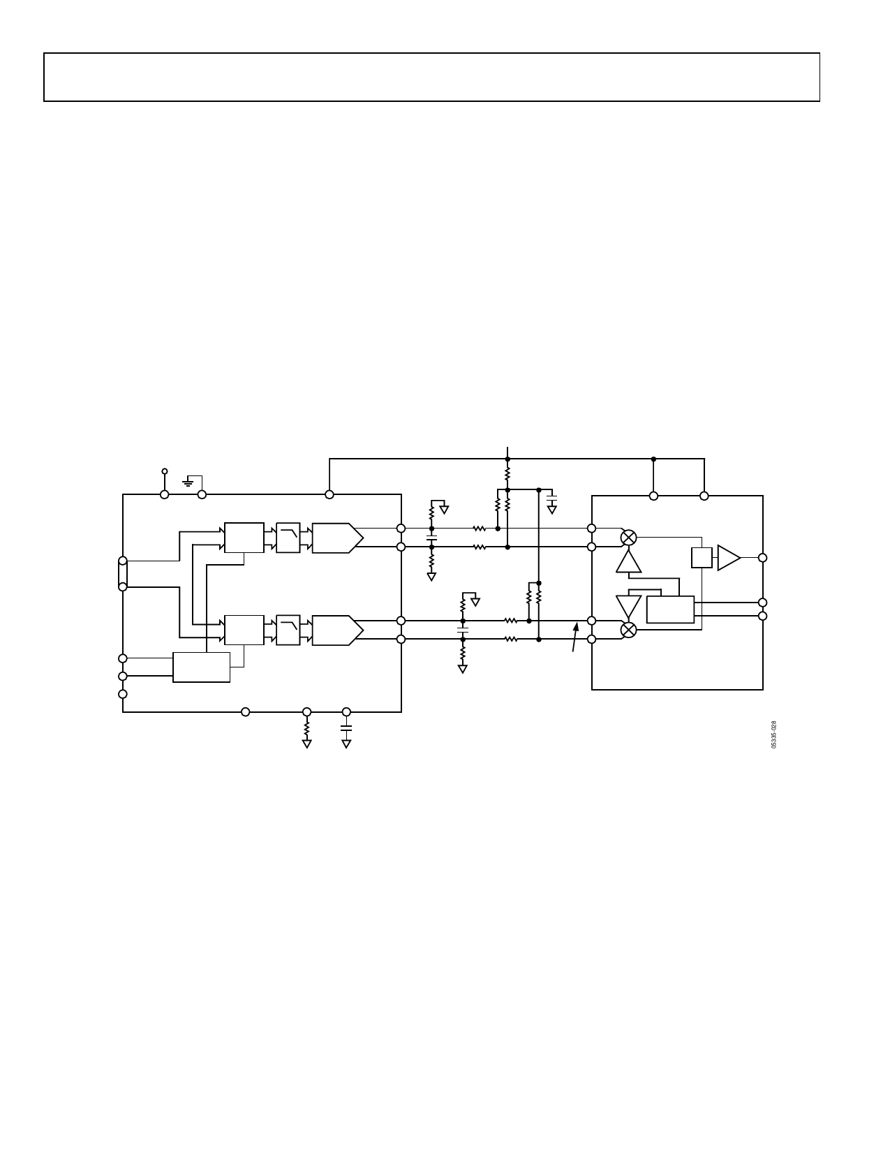
INTERFACE TO AD9761 TXDAC®
Figure 28 shows a dc-coupled current output DAC interface.
The use of dual-integrated DACs, such as the AD9761 with
specified ±0.02 dB and ±0.004 dB gain and offset matching
characteristics, ensures minimum error contribution (over
temperature) from this portion of the signal chain. The use of a
precision thin-film resistor network sets the bias levels precisely
to prevent the introduction of offset errors, which increase LO
feedthrough. For instance, selecting resistor networks with a
0.1% ratio matching characteristics maintains 0.03 dB gain and
offset matching performance.
Using resistive division, the dc bias level at the I and Q inputs
to the AD8346 is set to approximately 1.2 V. Each of the four
current outputs of the DAC delivers a full-scale current of
10 mA, giving a voltage swing of 0 V to 1 V (at the DAC
output). This results in a 0.5 V p-p swing at the I and Q inputs
of the AD8346 (resulting in a 1 V p-p differential swing).
Note that the ratio matching characteristics of the resistive
network, as opposed to its absolute accuracy, is critical in
preserving the gain and offset balance between the I and Q
signal path.
By applying small dc offsets to the I and Q signals from the
DAC, the LO suppression can be reduced from its nominal
value of −42 dBm to as low as −60 dBm while holding to
approximately −50 dBm over temperature (see Figure 12 for
a plot of LO feedthrough over temperature for an offset
compensated circuit).
5V
+5V
634Ω
DAC
DATA
INPUTS
DVDD DCOM
LATCH
I
SELECT
WRITE
LATCH
Q
MUX
CONTROL
CLOCK
SLEEP
AVDD
I
2×
DAC
AD9761
Q
2×
DAC
IOUTA
IOUTB
100Ω
100Ω
500Ω
500Ω
CFILTER
500Ω
500Ω
0.1μF
IBBP
IBBN
QOUTA
QOUTB
100Ω
100Ω
500Ω 500Ω
500Ω
QBBP
CFILTER
500Ω
QBBN
0.5V p-p EACH PIN
WITH VCM = 1.2V
FS ADJ REFIO
RSET
2kΩ
0.1μF
VPS1
VPS2
VOUT
Σ
PHASE
SPLITTER
LOIP
LOIN
AD8346
Figure 28. AD8346 Interface to AD9761 TxDAC
Rev. A | Page 12 of 20