74AHC1G02 Просмотр технического описания (PDF) - Philips Electronics
Номер в каталоге
Компоненты Описание
Список матч
74AHC1G02 Datasheet PDF : 16 Pages
| |||
Philips Semiconductors
2-input NOR gate
Product specification
74AHC1G02; 74AHCT1G02
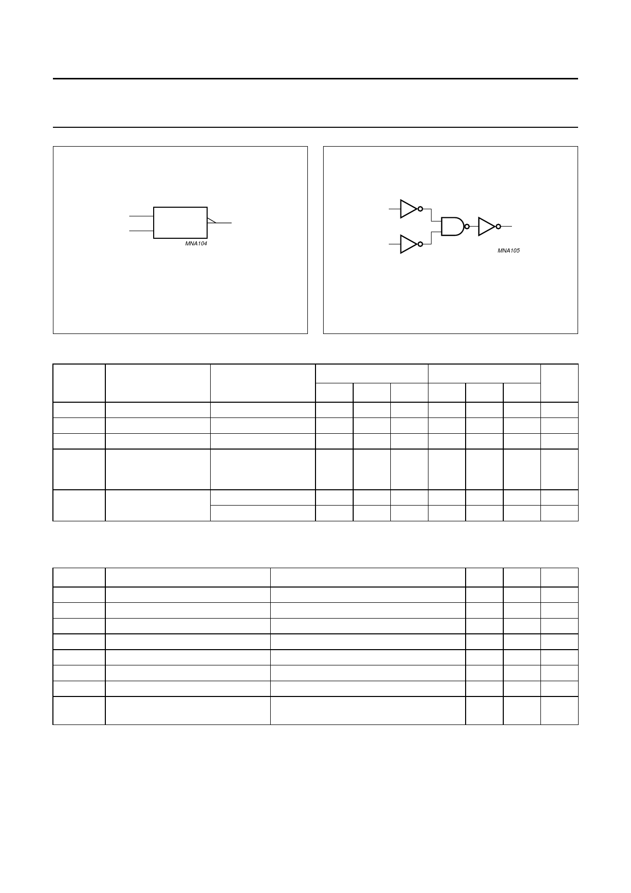
handbook, halfpage
1
2
≥1
4
MNA104
handbook, halfpageB
A
Y
MNA105
Fig.3 IEC logic symbol.
Fig.4 Logic diagram.
RECOMMENDED OPERATING CONDITIONS
SYMBOL
PARAMETER
VCC
VI
VO
Tamb
supply voltage
input voltage
output voltage
operating ambient
temperature
tr, tf
(∆t/∆f)
input rise and fall
times
CONDITIONS
see DC and AC
characteristics per
device
VCC = 3.3 ±0.3 V
VCC = 5 ±0.5 V
74AHC1G
74AHCT1G
UNIT
MIN. TYP. MAX. MIN. TYP. MAX.
2.0 5.0 5.5 4.5 5.0 5.5 V
0
−
5.5 0
−
5.5 V
0
−
VCC 0
−
VCC V
−40 +25 +125 −40 +25 +125 °C
−
−
100 −
−
−
ns/V
−
−
20
−
−
20
ns/V
LIMITING VALUES
In accordance with the Absolute Maximum Rating System (IEC 60134); voltages are referenced to GND (ground = 0 V).
SYMBOL
PARAMETER
VCC
supply voltage
VI
input voltage
IIK
input diode current
IOK
output diode current
IO
output source or sink current
ICC
VCC or GND current
Tstg
storage temperature
PD
power dissipation per package
CONDITIONS
VI < −0.5 V
VO < −0.5 or VO > VCC + 0.5 V; note 1
−0.5 V < VO < VCC + 0.5 V
for temperature range from
−40 to +125 °C
MIN.
−0.5
−0.5
−
−
−
−
−65
−
MAX.
+7.0
+7.0
−20
±20
±25
±75
+150
250
UNIT
V
V
mA
mA
mA
mA
°C
mW
Note
1. The input and output voltage ratings may be exceeded if the input and output current ratings are observed.
2002 May 27
4
Share Link: 