MB40968V Просмотр технического описания (PDF) - Fujitsu
Номер в каталоге
Компоненты Описание
Список матч
MB40968V Datasheet PDF : 18 Pages
| |||
MB40968/40968V
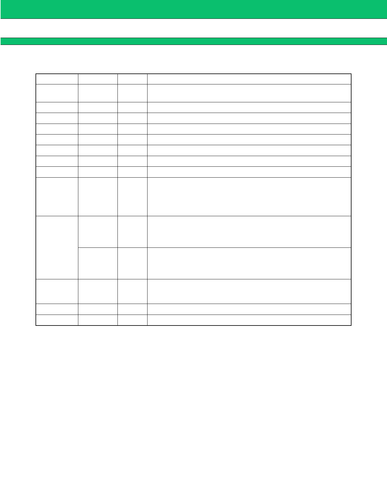
s PIN DESCRIPTION
Pin Number
25 to 28
1 to 4
6 to 13
5
14
24
19, 23
15
21
Symbol
A1 to A8
B1 to B8
CLKA
CLKB
VCCD
VCCA
D-GND
A-GND
18
VRIN
MB40968
VROUT
17
MB40968V
VROUT
16
COMP
22
AOUT
20
BOUT
I/O
Descriptions
I
A-channel Digital Signal Inputs: A1 (MSB), A8 (LSB)
I
B- channel Digital Signal Inputs: B1 (MSB), B8 (LSB)
I
A-channel Clock Input
I
B-channel Clock Input
— Power Supply for Digital Circuit
— Power Supply for Analog Circuit, two pins (19,23) should be used.
— Ground for Digital Circuit
— Ground for Analog Circuit
Terminal for reference voltage input.
Zero scale voltage of analog output is specified applying any voltage to
I
this terminal.
Input reference voltage should be 2.7 to 4.3V and,
VCCA – VRIN ≤ 2.2V
Terminal for reference voltage output by resistance-type potential
O
divider.
Analog output of “VCCA to 3/5 × VCCA” is supplied connecting this
terminal with VRIN terminal.
Terminal for reference voltage output consists of Band Gap reference.
O
This terminal supplies the voltage of “VCCA to VCCA – 2V”.
2V output is maintained connecting this terminal with VRIN, even if the
power supply fluctuates frequently.
Terminal for phase compensation capacitance;
— Capacitance of 1 µF or more should be inserted between COMP and A-
GND.
O A-channel Analog Signal Output
O B-channel Analog Signal Output
3
Share Link: 