AD74111 Просмотр технического описания (PDF) - Analog Devices
Номер в каталоге
Компоненты Описание
Список матч
AD74111 Datasheet PDF : 20 Pages
| |||
AD74111
1.125V
EXTERNAL
REFERENCE
REFCAP
Figure 9. External Reference
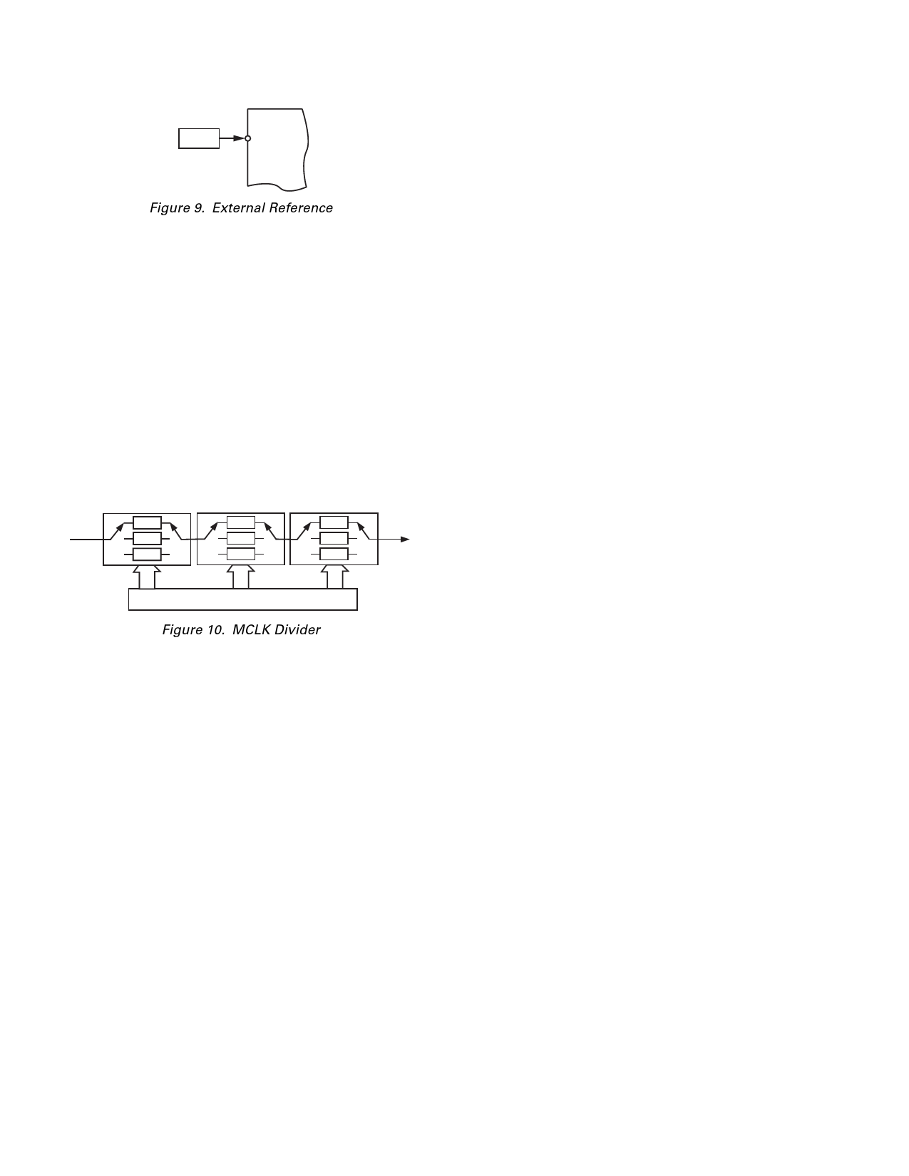
Master Clocking Scheme
The update rate of the AD74111’s ADC and DAC channels
requires an internal master clock (IMCLK) that is 256 times the
sample update rate (IMCLK = 256 ϫ fS). To provide some flex-
ibility in selecting sample rates, the device has a series of three
master clock prescalers that are programmable and allow the
user to choose a range of convenient sample rates from a single
external master clock. The master clock signal to the AD74111 is
applied at the MCLK pin. The MCLK signal is passed through
a series of three programmable MCLK prescaler (divider) circuits
that can be selected to reduce the resulting Internal MCLK
(IMCLK) frequency if required. The first and second MCLK
prescalers provide divider ratios of Ϭ1 (pass through), Ϭ2, Ϭ3;
while the third prescaler provides divider ratios of Ϭ1 (pass
through), Ϭ2, Ϭ4.
MCLK
PROGRAMMABLE MCLK DIVIDER
PRESCALER 1
PRESCALER 2
PRESCALER 3
/1
/1
/1
/2
/2
/2
/3
/3
/4
IMCLK
CONTROL REGISTER
Figure 10. MCLK Divider
The divider ratios allow a more convenient sample rate selection
from a common MCLK, which may be required in many voice
related applications. Control Register B should be programmed
to achieve the desired divider ratios.
Selecting Sample Rates
The sample rate at which the converter runs is always 256 times
the IMCLK rate. IMCLK is the Internal Master Clock and is the
output from the Master Clock Prescaler. The default sample rate
is 48 kHz (based on an external MCLK of 12.288 MHz). In this
mode, the ADC modulator is clocked at 3.072 MHz and the DAC
modulator is clocked at 6.144 MHz. Sample rates that are lower
than MCLK/256 can be achieved by using the MCLK prescaler.
Example 1: fSAMP = 48 kHz and 8 kHz Required
MCLK = 48 kHz ϫ 256 = 12.288 MHz to provide 48 kHz fSAMP.
For fSAMP = 8 kHz, it is necessary to use the Ϭ3 setting in
Prescaler 1, the Ϭ2 setting in Prescaler 2, and pass through
in Prescaler 3. This results in an IMCLK = 8 kHz ϫ 256 =
2.048 MHz (= 12.288 MHz/6).
Example 2: fSAMP = 44.1 kHz and 11.025 kHz Required
MCLK = 44.1 kHz ϫ 256 = 11.2896 MHz to provide 44.1 kHz fSAMP.
For fSAMP = 11.025 kHz, it is necessary to use the Ϭ1 setting in
Prescaler 1 and the Ϭ4 setting in Prescaler 2, and pass through
in Prescaler 3. This results in an IMCLK = 11.025 kHz ϫ 256
= 2.8224 MHz (= 11.2896 MHz/4).
Resetting the AD74111
The AD74111 can be reset by bringing the RESET pin low.
Following a reset, the internal circuitry of the AD74111 ensures
that the internal registers are reset to their default settings and
the on-chip RAM is purged of previous data samples. The DIN
pin is sampled to determine if the AD74111 is required to
operate in Master or Slave mode. The reset process takes 3072
MCLK periods, and the user should not attempt to program the
AD74111 during this time.
Power Supplies and Grounds
The AD74111 features three separate supplies: AVDD, DVDD1,
and DVDD2.
AVDD is the supply to the analog section of the device and must
be of sufficient quality to preserve the AD74111’s performance
characteristics. It is nominally a 2.5 V supply.
DVDD1 is the supply for the digital interface section of the device.
It is fed from the digital supply voltage of the DSP or controller
to which the device is interfaced and allows the AD74111
to interface with devices operating at supplies of between
2.5 V – 5% to 3.3 V + 10%.
DVDD2 is the supply for the digital core of the AD74111. It is
nominally a 2.5 V supply.
Accessing the Internal Registers
The AD74111 has seven registers that can be programmed to
control the functions of the AD74111. Each register is 10 bits
wide and is written to or read from using a 16-bit write or read
operation, with the exception of Control Register F, which is
read-only. Table V shows the format of the data transfer operation.
The Control Word is made up of a Read/Write bit, the register
address, and the data to be written to the device. Note that in a
read operation the data field is ignored by the device. Access to
the control registers is via the serial port through one of the
operating modes described below.
Serial Port
The AD74111 contains a flexible serial interface port that is
used to program and read the control registers and to send and
receive DAC and ADC audio data. The serial port is compatible
with many popular DSPs and can be programmed to operate in
a variety of modes, depending on which one best suits the DSP
being used. The serial port can be set to operate as a Master or
Slave device, as discussed below. Figure 11 shows a timing
diagram of the serial port.
–10–
REV. 0
Share Link: 