M38197 Просмотр технического описания (PDF) - MITSUBISHI ELECTRIC
Номер в каталоге
Компоненты Описание
Список матч
M38197 Datasheet PDF : 60 Pages
| |||
MITSUBISHI MICROCOMPUTERS
3819 Group
SINGLE-CHIP 8-BIT CMOS MICROCOMPUTER
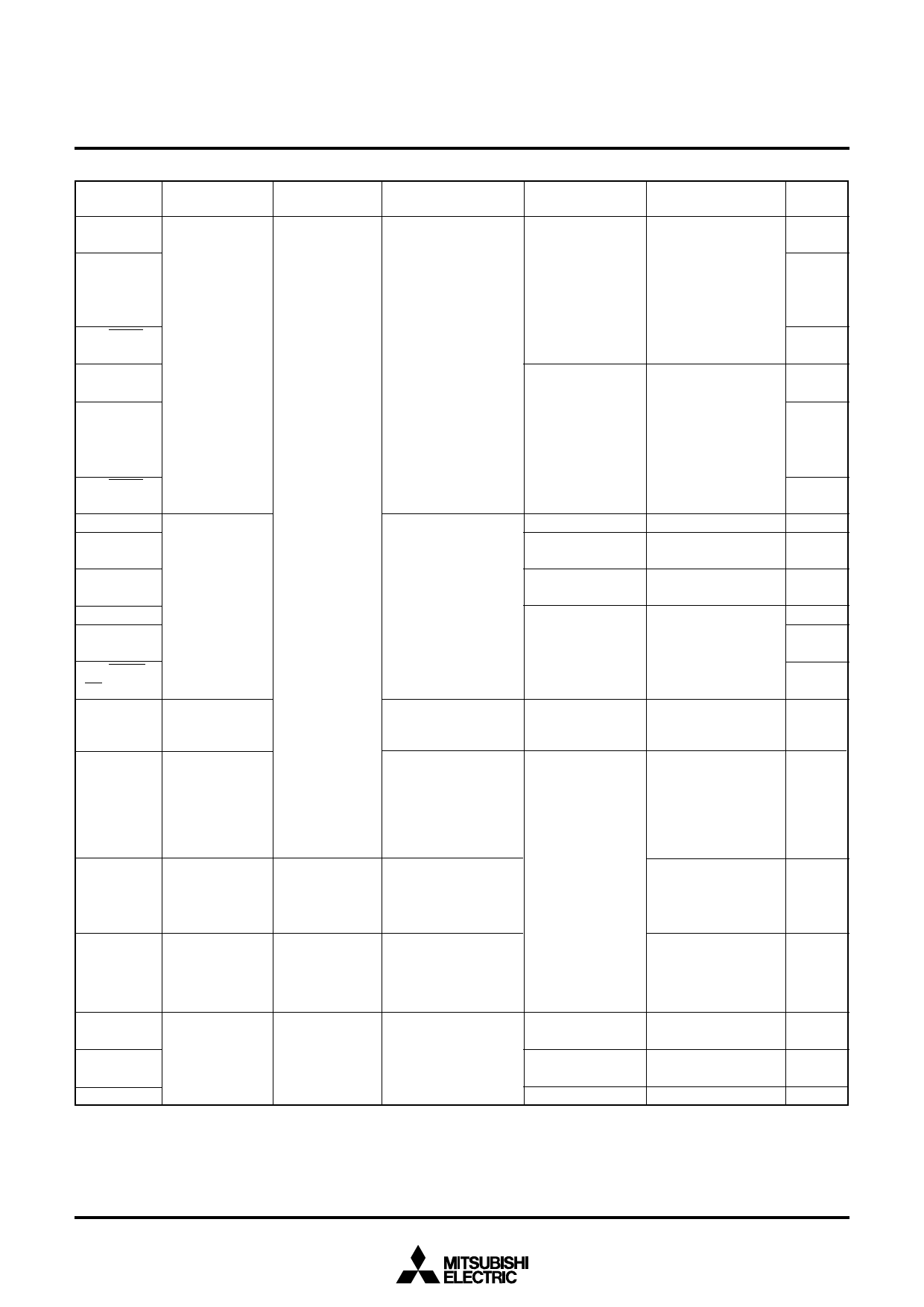
Pin
P50/SIN2/
AN8
P51/SOUT2/
AN9,
P52/SCLK2/
AN10
P53/SRDY2/
AN11
P54/SIN3/
AN12
P55/SOUT3/
AN13,
P56/SCLK3/
AN14
P57/SRDY3/
AN15
P60
P61/PWM
P62/CNTR0,
P63/CNTR1
P64/SIN1
P65/SOUT1,
P66/SCLK11
P67/SRDY1/
CS/SCLK12
P70/AN0–
P77/AN7
P80/SEG8–
P87/SEG15
P90/SEG16–
P97/SEG23
PA0/SEG0–
PA7/SEG7
PB0/XCOUT,
PB1/XCIN
PB2/DA
PB3
Name
Port P5
Port P6
Port P7
Port P8
Port P9
Port PA
Port PB
Input/Output
Input/output,
individual bits
Output
Input/output,
individual bits
Input/output,
individual bits
I/O Format
Non-Port Function
Related SFRS
Diagram
No.
(9)
Serial I/O2 func- Serial I/O2 control
tion I/O
register
(10)
A-D conversion in- AD/DA control regis-
put
ter
CMOS compatible
input level
(11)
CMOS 3-state output
(9)
Serial I/O3 func- Serial I/O3 control
tion I/O
register
A-D conversion in- AD/DA control regis-
(10)
put
ter
(11)
(4)
PWM (timer) out- Timer 56 mode regis-
put
ter
(8)
CMOS compatible
input level
Timer input
Interrupt edge selec-
tion register
(7)
CMOS 3-state output
Serial I/O1 control
(9)
Serial I/O1 func-
tion I/O
register
Serial I/O automatic
transfer control regis-
(10)
ter
(11)
CMOS compatible
input level
A-D conversion in- AD/DA control regis-
put
ter
(12)
CMOS 3-state output
CMOS compatible
input level
High-breakdown-
voltage P-channel
open-drain output
with pull-down
resistor
High-breakdown-
voltage P-channel
open-drain output
with pull-down
resistor
FLDC mode register
Segment/port switch (13)
register
FLD automatic
display function
FLDC mode register
(5)
CMOS compatible
input level
High-breakdown-
voltage P-channel
open-drain output
FLDC mode register
Segment/port switch (13)
register
CMOS compatible
I/O for sub-clock
generating circuit CPU mode register
(14)
(15)
input level
D-A conversion AD/DA control regis-
CMOS 3-state output output
ter
(16)
(4)
Note : Make sure that the input level at each pin is either 0 V or VCC during execution of the STP instruction. When an input level is at an intermediate poten-
tial, a current will flow from VCC to VSS through the input-stage gate.
11
Share Link: 